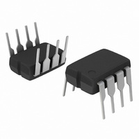
NCP1601APG ON Semiconductor, NCP1601APG Datasheet - Page 14

NCP1601APG
Manufacturer Part Number
NCP1601APG
Description
IC PFC CTRLR CRM/TRANSITION 8DIP
Manufacturer
ON Semiconductor
Datasheet
1.NCP1601APG.pdf
(19 pages)
Specifications of NCP1601APG
Mode
Critical Conduction (CRM), Discontinuous (Transition)
Frequency - Switching
58kHz
Current - Startup
17µA
Voltage - Supply
12.5 V ~ 18 V
Operating Temperature
-40°C ~ 125°C
Mounting Type
Through Hole
Package / Case
8-DIP (0.300", 7.62mm)
Switching Frequency
405 KHz
Maximum Operating Temperature
+ 125 C
Mounting Style
Through Hole
Minimum Operating Temperature
- 40 C
Lead Free Status / RoHS Status
Lead free / RoHS Compliant
Other names
NCP1601APGOS
Available stocks
Company
Part Number
Manufacturer
Quantity
Price
Company:
Part Number:
NCP1601APG
Manufacturer:
ON Semiconductor
Quantity:
1 200
Part Number:
NCP1601APG
Manufacturer:
ON/安森美
Quantity:
20 000
Figure 33 is studied. When the inductor current is exactly
zero (i.e., I
reached where R
the tolerance, the actual sense resistor R
higher than the ideal value of R
current signal is generated when sense current is smaller
than the ZCD threshold (i.e., I
between the operating and ideal ZCD points in Figure 33.
Hence, R
recommended value of R
R
greater than R
(eq.16) with different inductor currents I
studied.
Figure 34. When the inductor current I
I
the zero current signal is generated.
term is smaller the error or distance between the lines to the
line I
sense resistor R
possible to minimize the error in the zero current detection.
Overcurrent Protection (OCP)
I
is V
L(ZCD)
S(OCP)
S(ZCD)
Based on the CS pin (Pin 4) characteristics in Figure 15,
The higher value of R
Now that the R
These operating lines are added in Figure 33 to formulate
It is noted in Figure 34 and (eq.16) that when the (R
Overcurrent protection is reached when I
V
S(OCP)
S(ZCD)
Figure 34. CS Pin Characteristic with Different
L
ZCD
point
Best
, the sense current I
= 0 is smaller. Therefore, the value of the current
(200 mA typical). The offset voltage of the CS pin
which is 1 kΩ.
I L(OCP) =
S
L(ZCD)
(3.2 mV typical) in this condition. That is
has to be as low as possible. The best
V
S(ZCD)
R S > R S(ZCD) =
S
I
S(ZCD)
CS
S
= 0), the ideal ZCD point in the Figure is
is R
S
V S = R S − R CS I L
is also recommended to be as small as
Inductor Current
is set at a particular value which is
. From (eq.13), the operating lines in
I
R S I S(OCP) − V S(OCP)
L
S(ZCD)
= 0
S
S
S
I
is lower than I
L
is therefore the maximum of
(536 Ω typical). Considering
= I
makes the longer distance
S
R CS
L(ZCD)
S(ZCD)
< I
V S(ZCD)
I S(ZCD)
Operating
ZCD point
S(ZCD)
to ensure that zero
S
S(ZCD)
). That is,
L
L
is needed to be
S
I
of (eq.13) are
L
is lower than
is higher than
> I
L(ZCD)
and hence
(eq.15)
(eq.16)
(eq.17)
http://onsemi.com
I
S
CS
I
L
)
14
Drive Output of the device goes low.
Oscillator / Synchronization Block
to keep the operation in DCM or CRM only, the Drive
Output cannot turn on as long as there is some inductor
current flowing through the circuit. Hence, the zero current
signal is provided to the oscillator / synchronization block
in Figure 35. An input comparator monitors the Osc pin
(Pin 5) voltage and generates a clock signal. The negative
edge of the clock signal is stored in a RS latch. When zero
current is detected, the RS latch will be reset and a set signal
is sent to the output drive latch which turns on the MOSFET
in the PFC boost circuit. Figure 36 illustrates a typical
timing diagram of the oscillator block.
Oscillator Mode
C
typical), the pin sinks a current I
typical) and the external capacitor C
the voltage reaches V
a current I
C
propagation delay and the 3.5 V and 5 V threshold
conditions are measured on 220 pF C
the actual oscillator hysteresis is a slightly smaller.
Osc
(latch set signal)
Drive output
Clock edge
Osc clock
osc
osc
When overcurrent protection threshold is reached, the
The NCP1601 is a DCM / CRM PFC controller. In order
The Osc pin (Pin 5) is connected to an external capacitor
Figure 37. Oscillator Mode Timing Diagram in DCM
Osc pin
voltage
(DCM)
(latch output)
. When the voltage of this pin is above V
is charged. It is noted that there is a typical 300 ns
5
clock edge
Figure 35. Oscillator / Synchronization Block
clock latch
Figure 36. Oscillator Block Timing Diagram
Discontinuous mode
inductor
45 mA
94 mA
current
clock
och
0
(45 mA typical) and the external capacitor
1
5 V/3.5 V
Oscillator Clock
sync(L)
+
- -
(3.5 V typical), the pin sources
Critical mode
odch
S
R
Zero Current
osc
osc
Q
delay
(94 – 45 = 49 mA
discharges. When
capacitor. Hence,
&
sync(H)
Turn on
MOSFET
3.5 V
5 V
(5 V
time


