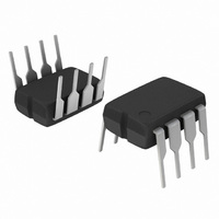
NCP1601BPG ON Semiconductor, NCP1601BPG Datasheet

NCP1601BPG
Specifications of NCP1601BPG
Available stocks
Related parts for NCP1601BPG
NCP1601BPG Summary of contents
Page 1
NCP1601A, NCP1601B Compact Fixed Frequency Discontinuous or Critical Conduction Voltage Mode Power Factor Correction Controller The NCP1601 is a controller designed for Power Factor Correction (PFC) boost circuits. The device operates in fixed- - frequency Discontinuous Conduction Mode (DCM) and ...
Page 2
EMI AC Filter Input AC EMI Input Filter Current Mirror CC(on UVLO & Shutdown / ...
Page 3
PIN FUNCTION DESCRIPTION Pin Symbol Function 1 FB Feedback / This pin receives a current I Shutdown for the output regulation, output Overvoltage Protection (OVP), and output undervoltage protection (UVP). When I When Control The voltage of ...
Page 4
MAXIMUM RATINGS Rating FB Ramp, CS, Osc Pins (Pins 1- -5) control Maximum Voltage Range Maximum Current Drive Output (Pin 7) Maximum Voltage Range Maximum Current Range (Note 2) Power Supply Voltage (Pin 8) Maximum Voltage Range Maximum ...
Page 5
ELECTRICAL CHARACTERISTICS V = 100 nF, Ramp = 100 pF, Osc = 220 pF unless otherwise specified) control Characteristic OSCILLATOR Oscillator Frequency (Osc = 220 pF to GND) Internal Capacitance of the Oscillator Pin Maximum Oscillator Switching Frequency Oscillator Discharge ...
Page 6
ELECTRICAL CHARACTERISTICS V = 100 nF, Ramp = 100 pF, Osc = 220 pF unless otherwise specified) control Characteristic SUPPLY SECTION Startup Threshold (UVLO) – NCP1601A Startup Threshold (UVLO) – NCP1601B Minimum Voltage for Operation After Turn- -On UVLO Hysteresis ...
Page 7
T , JUNCTION TEMPERATURE (C) J Figure 7. Reference Current vs. Temperature 100 ...
Page 8
T , JUNCTION TEMPERATURE (C) J Figure 13. Overvoltage Protection Threshold vs. Temperature 120 100 125 C ...
Page 9
T , JUNCTION TEMPERATURE (C) J Figure 19. Zero Current Sense Resistor vs. Temperature 12.0 11.5 11.0 10.5 10.0 9.5 9 ...
Page 10
Introduction The NCP1601 is a Power Factor Correction (PFC) boost controller designed to operate Conduction Mode (DCM) and Critical Conduction Mode (CRM). The fixed- - frequency nature of DCM limits the maximum switching frequency. It limits the possible conducted and ...
Page 11
filter Figure 26. DCM/CRM PFC Boost Converter PFC Methodology NCP1601 uses a proprietary PFC methodology ...
Page 12
V ton = V control It is noted that V is always greater than or equal to ton V (i.e., V control ton control In summary, the input impedance Z from (eq.1)- - (eq. ...
Page 13
Figure 31. On the other hand, the V in the low V condition is much higher than the high V ac condition. In order to not over- - design the ...
Page 14
Based on the CS pin (Pin 4) characteristics in Figure 15, Figure 33 is studied. When the inductor current is exactly zero (i.e 0), the ideal ZCD point in the Figure is L(ZCD) reached where ...
Page 15
There is an internal capacitance C osc(int) in the oscillator pin and the oscillator frequency (405 kHz typical) when the Osc pin is opened. osc(max) Hence, the oscillator switching frequency can be formulated in (eq.18) and represented ...
Page 16
... Vac SPF47283900 Figure 40. 130 W Power Factor Correction Circuit ORDERING INFORMATION Device NCP1601APG NCP1601ADR2G NCP1601BPG NCP1601BDR2G †For information on tape and reel specifications, including part orientation and tape sizes, please refer to our Tape and Reel Packaging Specifications Brochure, BRD8011/D. KBP06 450 mH / 4.5 A 680 k ...
Page 17
Appendix I – Summary of Equations in NCP1601 Boost PFC Description Boost converter V out → V out − out Input current averaged filter ...
Page 18
... B S 0.25 (0.010 SEATING PLANE - - 0.25 (0.010 *For additional information on our Pb- -Free strategy and soldering details, please download the ON Semiconductor Soldering and Mounting Techniques Reference Manual, SOLDERRM/D. PACKAGE DIMENSIONS SOIC SUFFIX CASE 751--07 ISSUE 0.10 (0.004 SOLDERING FOOTPRINT* 1.52 0.060 7.0 4.0 ...
Page 19
... SCILLC is an Equal Opportunity/Affirmative Action Employer. This literature is subject to all applicable copyright laws and is not for resale in any manner. PUBLICATION ORDERING INFORMATION LITERATURE FULFILLMENT: Literature Distribution Center for ON Semiconductor P.O. Box 5163, Denver, Colorado 80217 USA Phone: 303- -675- -2175 or 800- -344- -3860 Toll Free USA/Canada Fax: 303- -675- -2176 or 800- -344- -3867 Toll Free USA/Canada Email: orderlit@onsemi ...


