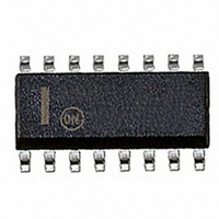
NCP1651DR2G ON Semiconductor, NCP1651DR2G Datasheet - Page 18

NCP1651DR2G
Manufacturer Part Number
NCP1651DR2G
Description
IC PFC CONTROLLER CCM/DCM 16SOIC
Manufacturer
ON Semiconductor
Datasheet
1.NCP1651DR2G.pdf
(32 pages)
Specifications of NCP1651DR2G
Mode
Continuous Conduction (CCM), Discontinuous Conduction (DCM)
Frequency - Switching
250kHz
Current - Startup
8.5mA
Voltage - Supply
10 V ~ 18 V
Operating Temperature
-40°C ~ 125°C
Mounting Type
Surface Mount
Package / Case
16-SOIC (3.9mm Width)
Switching Frequency
25 KHz to 250 KHz
Maximum Operating Temperature
+ 125 C
Mounting Style
SMD/SMT
Minimum Operating Temperature
- 40 C
Lead Free Status / RoHS Status
Lead free / RoHS Compliant
Other names
NCP1651DR2GOS
NCP1651DR2GOS
NCP1651DR2GOSTR
NCP1651DR2GOS
NCP1651DR2GOSTR
Available stocks
Company
Part Number
Manufacturer
Quantity
Price
Part Number:
NCP1651DR2G
Manufacturer:
ON/安森美
Quantity:
20 000
DC Reference and Buffer
with a nominal output voltage of 4.0 volts. It is temperature
compensated, and trimmed for a 1% tolerance of its
nominal voltage, with an overall tolerance of 2%. To
assure maximum stability, this is only used as a reference so
there is minimal loading on this source.
which creates a 6.5 volt supply. This is used as an internal
voltage to power many of the blocks inside of the NCP1651
and is also available for external use. The 6.5 volt reference
is designed to be terminated with at 0.1 mF capacitor for
stability reasons.
6.5 volt supply, so care should be used when connecting
external loads. A short or overload on this voltage output
will inhibit the operation of the chip.
Undervoltage Lockout
assure that the unit does not exhibit undesirable behavior at
low V
that allows rapid charging of the V
hold the unit off, and in a low bias current mode until the V
voltage reaches a nominal 10.8 volt level. At this point the
unit will begin operation, and the UVLO will no longer be
active. If the V
below the turn- -on point, the UVLO circuit will again
become active.
removes power from all internal circuitry by shutting off the
6.5 volt supply. The 4.0 volt reference remains active, and
the UVLO and Shutdown comparators are also active.
Multiplier
Reference multiplier. This innovative design allows greatly
improved accuracy compared to a conventional linear
analog multiplier. The multiplier uses a PWM switching
circuit to create a scalable output signal, with a very well
defined gain.
(V- -I) converter. By converting the input voltage into a
current, an overall multiplier gain can be accomplished. In
addition, there will be no error in the output signal due to the
series rectifier.
comparator. This selects a pulse width for the comparator
output. The current signal from the V- -I converter is factored
by the duty cycle of the PWM comparator, and then filtered
by the RC network on the output. This network creates a low
pass filter, and removes the high frequency content from the
original waveform.
The internal DC reference is a precision bandgap design
The DC reference is fed into a buffer with a gain of 1.625
There is no buffer between the internal and external
An Undervoltage Lockout circuit (UVLO) is provided to
When the V
When in the active (shutdown) state, the UVLO circuit
The NCP1651 uses a new proprietary concept for its
One input (A) to the multiplier is a voltage- -to- -current
The other signal (Input P) is input into the PWM
CC
levels. It also reduces power consumption to a level
CC
CC
cap is initially charging, the UVLO will
voltage falls to a level that is 1.0 volts
CC
cap.
OPERATING DESCRIPTION
http://onsemi.com
CC
18
and is the same signal as is used in the PWM. It will therefore
have the same frequency as the power stage.
to be a DC signal, low frequency AC signals (relative to the
ramp frequency) work well also.
current- -to- -voltage ratio of the V- -I converter, the load
resistor of the output filter and the peak and valley points of
the sawtooth ramp. When the P input signal is at the peak of
the ramp waveform, the comparator will allow the A input
signal to pass without chopping it at all. This gives an output
voltage of the A current multiplied by the output filter
resistance. When the P input signal is at the ramp valley
voltage, the comparator is held low and no current is passed
into the output filter. In between these two extremes, the duty
cycle (and therefore, the output signal) is proportional to the
level of the P input signal.
network needs to be greater than twice the highest line
frequency (120 Hz for a 60 Hz line), and less than the
switching frequency. A recommended starting point is a
factor of 20 to 50 less than the switching frequency.
a 2.0 kHz pole is a good starting point. This would be a factor
of 50 below the switching frequency, and is still far enough
above the 120 Hz rectified line frequency that it won’t cause
undesirable distortion.
INPUT P
The multiplier ramp is generated by the internal oscillator,
It is not necessary for Input P (into the PWM comparator)
The gain of the multiplier is determined by the
The output filter is a parallel RC network. The pole for this
The pole is calculated by the formula:
So, for a 60 Hz line, and a 100 kHz switching frequency,
Inverting Input
RAMP
Figure 32. Simplified Multiplier Schematic
+
--
f o =
2 × π × R × C
CONVERTER
FB/SD
V to I
1
A
OUTPUT


