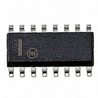
NCP1651DR2G ON Semiconductor, NCP1651DR2G Datasheet - Page 26

NCP1651DR2G
Manufacturer Part Number
NCP1651DR2G
Description
IC PFC CONTROLLER CCM/DCM 16SOIC
Manufacturer
ON Semiconductor
Datasheet
1.NCP1651DR2G.pdf
(32 pages)
Specifications of NCP1651DR2G
Mode
Continuous Conduction (CCM), Discontinuous Conduction (DCM)
Frequency - Switching
250kHz
Current - Startup
8.5mA
Voltage - Supply
10 V ~ 18 V
Operating Temperature
-40°C ~ 125°C
Mounting Type
Surface Mount
Package / Case
16-SOIC (3.9mm Width)
Switching Frequency
25 KHz to 250 KHz
Maximum Operating Temperature
+ 125 C
Mounting Style
SMD/SMT
Minimum Operating Temperature
- 40 C
Lead Free Status / RoHS Status
Lead free / RoHS Compliant
Other names
NCP1651DR2GOS
NCP1651DR2GOS
NCP1651DR2GOSTR
NCP1651DR2GOS
NCP1651DR2GOSTR
Available stocks
Company
Part Number
Manufacturer
Quantity
Price
Part Number:
NCP1651DR2G
Manufacturer:
ON/安森美
Quantity:
20 000
Error Amplifier
circuit, and therefore is not part of the chip. A minimal
solution would include either a discrete amplifier and
reference, or an integrated circuit that combines both, such
as the TL431 series of regulators.
low cost regulator, however, due to the slow loop response
of a PFC regulator it will not protect against overvoltage
conditions (e.g. load removal) or droop when a transient
load is added.
PFC controller will operate at maximum duty cycle with the
optocouple in a non- -conducting state. This is necessary to
allow the unit to bring up the output when the system is
initially energized. At this time there is not output voltage
available to drive the LED in the optocoupler.
need to be rated at the maximum voltage that the output will
experience, including transient conditions. Resistors R
and R
equal to V
a current limiting resistor that protects the optocoupler from
current transients due to output surges.
transients. Since the bandwidth of the error amplifier is very
low, its output can not respond rapidly to changes in the
output voltage. A transient change in the output voltage will
change the current through R
error amplifier does not change immediately, if the output
voltage increases, the voltage across R
This drives more current through the optocoupler, which in
turn reduces the output of the converter.
slightly more expensive, and offers excellent protection
from positive transients, and quick recovery from negative
transients.
V
V
The error amplifier resides on the secondary side of the
This configuration for the error amplifier will result in a
The primary side circuit has been designed such that the
In the circuit of Figure 41, the amplifier and reference
This design also includes inherent compensation from
An alternate regulator is recommended, which is only
out
R
R
dc2
dc1
dc2
R
need to be chosen such that the voltage at V is
V
ref2
fb
ref2
Figure 41. Error Amplifier Circuit
when V
C
fb
+
--
Error
Amp
out
is at its regulated voltage. R
R
opto
opto
. Since the output of the
opto
will increase.
FB/SD
http://onsemi.com
opto
dc1
is
26
error amplifier with slow loop response, plus overvoltage
and undervoltage comparators. Under normal operation the
outputs of the Undervoltage and Overvoltage Comparators
are high. The Undervoltage Comparator provides drive for
the optocoupler, while the Overvoltage Comparator reverse
biases the diode on its output and is out of the loop.
below the regulation limit. If an overvoltage condition
exists, the Overvoltage comparator will respond very
quickly. When its output goes low, it will provide maximum
drive to the optocoupler, which will shut off the output of the
converter.
level, the Undervoltage Comparator will go low. This will
remove the drive from the optocoupler, which will allow the
regulator to increase the duty cycle and return the output to
its regulation range much faster than the error amplifier
could.
with the appropriate changes in R
R
R
R
drive the optocoupler. If additional current is needed, change
the 2 in the denominator of that equation to the current
(in mA) that is desired.
out
bias
opto
The configuration shown in Figure 42, incorporates an
This circuit is designed with 8% trip points both above and
If the output voltage drops 8% or more below its regulated
This configuration will work over a range of 5 to 30 volts,
The value for R
C
(kΩ) = (V
(kΩ) = (V
(kΩ) = (V
out
Figure 42. Error Amp with Over/Undershoot
5.23 k
453
422
out
out
out
9.31 k
R
opto
out
- - 4.753) / 0.7785
- - 4.4)
- - 3) / 2
Error Amplifier
Undervoltage
Overvoltage
Comparator
will allow a maximum of 2 mA to
Capacitor
+
--
--
+
--
+
Protection
MC3303
4.02 k
5.23 k
out
, R
R
3.6 k
opto
0.01 mF
bias
and R
R
7.5 k
bias
opto
12 V
TL431
.
R
tn


