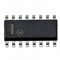
NCP1651DR2G ON Semiconductor, NCP1651DR2G Datasheet - Page 28

NCP1651DR2G
Manufacturer Part Number
NCP1651DR2G
Description
IC PFC CONTROLLER CCM/DCM 16SOIC
Manufacturer
ON Semiconductor
Datasheet
1.NCP1651DR2G.pdf
(32 pages)
Specifications of NCP1651DR2G
Mode
Continuous Conduction (CCM), Discontinuous Conduction (DCM)
Frequency - Switching
250kHz
Current - Startup
8.5mA
Voltage - Supply
10 V ~ 18 V
Operating Temperature
-40°C ~ 125°C
Mounting Type
Surface Mount
Package / Case
16-SOIC (3.9mm Width)
Switching Frequency
25 KHz to 250 KHz
Maximum Operating Temperature
+ 125 C
Mounting Style
SMD/SMT
Minimum Operating Temperature
- 40 C
Lead Free Status / RoHS Status
Lead free / RoHS Compliant
Other names
NCP1651DR2GOS
NCP1651DR2GOS
NCP1651DR2GOSTR
NCP1651DR2GOS
NCP1651DR2GOSTR
Available stocks
Company
Part Number
Manufacturer
Quantity
Price
Part Number:
NCP1651DR2G
Manufacturer:
ON/安森美
Quantity:
20 000
Current Scaling Resistor & Filter Capacitor
current sense amplifier which is fed into the AC error
amplifier. R
level for protection purposes in the AC error amplifier
circuit.
signal at the input to the AC error amplifier to less than
4.5 volts at low line and full load. 4.5 volts is the clamp
voltage at the output of the reference amplifier and limits the
maximum averaged current that the unit can process. The
equation for R
Where: P
Where:
Where:
Where:
be advisable to increase the input power to assure operation
at maximum power over production tolerance variations.
its pole about a factor of 10 below the switching frequency.
Where: C
Where:
so, for a 100 kHz switching frequency, a 10 kHz pole is
desirable, and C
Reference Multiplier
modulated representation of the analog input. The multiplier
is internally loaded with a resistor to ground which will set
the DC gain. An external capacitor is required to filter the
signal back into one that resembles the input fullwave
rectified sinewave. The pole for this circuit should be greater
than the line frequency and lower than the switching
frequency.
starting value for a 60 Hz line frequency. The filter capacitor
for pin 10 can be determined by the following equation:
Where: C
Where:
R
R
This equation does not allow for tolerances, and it would
The current sense filter capacitor should be selected to set
The output of the reference multiplier is a pulse width
1/15th of the switching frequency is a recommended
7
7
R 7 =
sets the gain of the averaged current signal out of the
should be calculated to limit the maximum current
R
V
AC
f = pole frequency (kHz)
f
pole
in
S
inLL
6
10
Vin LL
7
= Shunt resistance (W)
= Pin 6 capacitance (nF)
ratio
= rated input power (W)
C 10 =
= Pin 10 capacitance (F)
is used to scale the current to the appropriate
= Ref gain pole freq (Hz)
7
= min. operating rms input voltage (W)
is:
6
= AC attenuation factor at pin 9
would be 0.5 nF.
4.5 − (0.75 ⋅ AC ratio ⋅ Vin LL ⋅ 2
2 3.14 25 k f pole
212 k ⋅ R S ⋅ P in
C 6 = 5.3
1
f
= 6.366E--6
f pole
)
http://onsemi.com
28
AC Error Amplifier
that is terminated with a series R
a pole- -zero pair.
look at the two signals that reach the PWM inputs. The
non- -inverting input is a slow loop using the averaged
current signal. It’s gain is:
amplifier averaging circuit. The next term is the gain of the
transconductance amplifier and the constant is the gain of
the AC Reference Buffer.
current signal to the PWM non- -inverting input. This gain is
16 k/3 k = 5.33, since the input signal is converted to a
current through a 3 k resistor in the current sense amplifier,
and then terminated by the 16 k resistor at the PWM input.
less than the gain of the high frequency path. This can be
written as:
The suggested resistor and capacitor values are:
and for a zero at 1/10th of the switching frequency
Where: R
Where:
Where:
Where:
The AC error amplifier is a transconductance amplifier
To determine the values of R
Where the first two terms are the gains in the current sense
The high frequency path is that of the instantaneous
For stability, the gain of the low frequency path must be
g
C
f
sw
m
7
11
A If =
& R
is in units of mhos
is in Hz
is in Farads
11
345, 000 ⋅ g m ⋅ R 11
30 k
3 k
are in units of Ohms
R 11 =
C 11 =
⋅
15 k
R 7
R 7
130,000 g m
f SW R 11
⋅ (g m ⋅ R 11 ) ⋅ 2.3
1.59
3
R 7
C
and C
impedance. This creates
< 5.3
3
, it is necessary to


