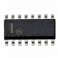
NCP1651DR2G ON Semiconductor, NCP1651DR2G Datasheet - Page 29

NCP1651DR2G
Manufacturer Part Number
NCP1651DR2G
Description
IC PFC CONTROLLER CCM/DCM 16SOIC
Manufacturer
ON Semiconductor
Datasheet
1.NCP1651DR2G.pdf
(32 pages)
Specifications of NCP1651DR2G
Mode
Continuous Conduction (CCM), Discontinuous Conduction (DCM)
Frequency - Switching
250kHz
Current - Startup
8.5mA
Voltage - Supply
10 V ~ 18 V
Operating Temperature
-40°C ~ 125°C
Mounting Type
Surface Mount
Package / Case
16-SOIC (3.9mm Width)
Switching Frequency
25 KHz to 250 KHz
Maximum Operating Temperature
+ 125 C
Mounting Style
SMD/SMT
Minimum Operating Temperature
- 40 C
Lead Free Status / RoHS Status
Lead free / RoHS Compliant
Other names
NCP1651DR2GOS
NCP1651DR2GOS
NCP1651DR2GOSTR
NCP1651DR2GOS
NCP1651DR2GOSTR
Available stocks
Company
Part Number
Manufacturer
Quantity
Price
Part Number:
NCP1651DR2G
Manufacturer:
ON/安森美
Quantity:
20 000
Loop Model
six sections. The voltage divider, error amplifier, and opto
Transfer are external to the chip, and the reference signal,
modulator and output stage are internal.
simplified based on the assumption that that poles and zeros
in the current feedback loop are considerably greater than
the bandwidth of the overall loop. This should be a good
assumption, because a bandwidth in the kilohertz is
necessary for a good current waveform, and the voltage error
amplifier needs to have a bandwidth of less than the lowest
line frequency that will be used.
pole that varies with the load. The pole on the voltage error
amplifier will be determined by this analysis.
Voltage Divider
circuitry. It is a simple resistive divider that reduces the
output voltage to the level required by the internal reference
on the voltage error amplifier. If the amplifier circuit of
Figure 42 is used, there are four resistors instead of 2. To
determine the gain of this circuit, R
the upper two resistors, 9.31 k and 453 Ohms respectively,
and R
5.23 k respectively.
V
V o
V′
The model for the voltage loop has been broken down into
The modulator and output stage circuitry is greatly
There are two poles in this circuit. The output filter has a
The voltage divider is located on the secondary side
=
R
R
DIVIDER
dc1
V
dc2
R dc1 + R dc2
dc2
ref2
R
R dc2
fb
is the equivalent of the lower two resistors, 422 and
+
--
C
ERROR
fb
AMP
for f > f
for f < f
A v =
V
R
f z =
A v = R fb ∕R dc1
ea
opto
ERROR AMP
z
z
:
:
2 π f C fb R dc1
2 π C fb R fb
1
1
V
fb
FB/SD
C
dc1
0.022 mF
8
ΔV ea
8
OPTO TRANSFER
ΔV fb
is the equivalent of
6.5 V
=
Figure 43. Voltage Regulation Loop
3.8 k CTR
3.8 k
R opto
REFERENCE
MULTIPLIER
Loop Compensation
http://onsemi.com
25 k
Ref Fltr
REFERENCE SIGNAL
V ac =
ΔV ref
ΔV fb
V
29
R ac1 + R ac2
V
ref
ac
V line R ac2
= 2.66 V ac
10
R
C
ac2
10
Voltage Error Amplifier
equations. When this amplifier is compensated with a
pole- -zero pair, there will be a unity gain pole which will be
cancelled by the zero at frequency f
bode plot would be:
R
calculated using the formula for f
fb
ERROR
--20
The voltage error amplifier is constrained by the two
The gain at frequencies greater than f
AMP
20
. Once R
AC
--
+
0
4 V
Unity Gain
R
ac1
fb
ΔV ref
Figure 44. Pole- -zero Bode Plot
ΔI in
I
C.S. Amp
avg
+
--
is determined, the value of C
=
PWM
MODULATOR AND OUTPUT STAGE
R S 75, 000
7
R
7
R 7
f, FREQUENCY
LOGIC
V
line
ΔV out
ΔI in
z
=
I
OUT
1
5
S+
.
f p =
N p
N s
z
2 π R L C
. The corresponding
η R L
1
z
Q1
f
z
is determined by
N
T − t on
fb
p
R
t on
: N
S
can be easily
I
in
s
A
V
C
V
R
o
L


