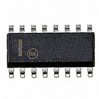
NCP1651DR2G ON Semiconductor, NCP1651DR2G Datasheet - Page 30

NCP1651DR2G
Manufacturer Part Number
NCP1651DR2G
Description
IC PFC CONTROLLER CCM/DCM 16SOIC
Manufacturer
ON Semiconductor
Datasheet
1.NCP1651DR2G.pdf
(32 pages)
Specifications of NCP1651DR2G
Mode
Continuous Conduction (CCM), Discontinuous Conduction (DCM)
Frequency - Switching
250kHz
Current - Startup
8.5mA
Voltage - Supply
10 V ~ 18 V
Operating Temperature
-40°C ~ 125°C
Mounting Type
Surface Mount
Package / Case
16-SOIC (3.9mm Width)
Switching Frequency
25 KHz to 250 KHz
Maximum Operating Temperature
+ 125 C
Mounting Style
SMD/SMT
Minimum Operating Temperature
- 40 C
Lead Free Status / RoHS Status
Lead free / RoHS Compliant
Other names
NCP1651DR2GOS
NCP1651DR2GOS
NCP1651DR2GOSTR
NCP1651DR2GOS
NCP1651DR2GOSTR
Available stocks
Company
Part Number
Manufacturer
Quantity
Price
Part Number:
NCP1651DR2G
Manufacturer:
ON/安森美
Quantity:
20 000
Optocoupler Transfer
the error signal from the secondary to primary side circuits.
The gain is based on the Current Transfer Ratio of the
device. This can change over temperature and time, but will
not result in a large change in dB.
capacitor is used, the pole may become low enough that it
will have an effect on the gain phase plots near the unity gain
crossover frequency. In this case and additional zero will be
required in the error amplifier bias circuitry.
Reference Signal
via. the optocoupler, is converted to a current by the V- -I
converter and is then used as an input to the reference
multiplier. The gain of this block is dependent on the AC
input voltage, because of the multiplier which requires two
inputs for one output.
Modulator and Output Stage
multiplier and forces the current to follow the shape and
amplitude. The is an internal loop within this section due to
the current sense amplifier. Based on the assumptions listed
in the introduction to this analysis, this is not analyzed
separately.
the pole. There is a single pole due to the output filter. Since
the NCP1651 is a current mode converter, the inductor is not
part of the output pole as can be seen in that equation.
been split into two sets of equations. The first defines the
relationship between the input current and AC reference
signal, and the later, define the output stage gain and pole.
Due to the nature of a flyback transformer, the gain of the
output stage is dependant on the duty cycle (t
continuous mode operation, the on- -time is:
Calculating the Loop Gain
involved in this calculation have been determined with the
exception of the pole- -zero pair on the output of the voltage
error amplifier.
necessary to convert these to the decibel format using the
following formula:
A(dB) = 20 Log
A(dB) = 20 Log
The optocoupler is used to allow for galvanic isolation for
The recommended capacitor at pin 8 is 0.022 mF. If a larger
The error signal is transmitted to the primary side circuit
The modulator receives an input from the reference
The equation for the gain is good for frequencies below
The modulator and output stage transfer functions have
At this point in the design process, all of the parameters
All equations give gains in absolute numbers. It is
For example, the voltage divider would be:
A =
10
10
t on =
(A)
0.0099 = - -40 dB
560 k + 5.6 k
5.6 k
N S
N P
⋅
⋅ V rms
2
V out
T
= 0.0099
+ 1
on
/T). For
http://onsemi.com
30
It is recommended that the compensation for the error
amplifier be calculated under high line, full load conditions.
This should be the greatest bandwidth that the unit will see.
PFC unit, must be less than the line frequency. If the
bandwidth approaches or exceeds the line frequency, the
voltage error amplifier signal will have frequency
components in its output that are greater than the line
frequency. These components will cause distortion in the
output of the reference amplifier, which is used to shape the
current waveform. This in turn will cause distortion in the
current and reduce the power factor.
converter is 10 Hz, and slightly less for a 50 Hz system. This
can be adjusted to meet the particular requirements of a system.
The unity gain bandwidth is determined by the frequency at
which the loop gain passes through the 0 dB level.
with a slope of - -20 dB for approximately on decade on either
side of the unity gain frequency. This assures a phase margin
of greater than 45.
of Figure 18 as follows:
Divider: Calculate V/V
will not change with frequency.
Optocoupler Transfer: Calculate V
provided. Convert this value into dB.
Reference Signal: Calculate V
the AC input signal at high line that will be seen on pin 9.
Convert this to dB. This is also a constant value.
Modulator and Output Stage: Calculate the gain in dB for
DI
output stage (DV
gain will be constant for all frequencies less than f
at the pole frequency, this gain will drop off at a rate of
20 dB/decade.
include the output pole. It should resemble the plot of
Figure 45. This plot shows a gain of 34 dB until the pole of
the output filter is reached at 3 Hz. After that, the gain is
reduced at a rate of 20 dB/decade.
The gain of the loop will vary as the input voltage changes.
By necessity, the unity gain (0 dB) loop bandwidth for a
Typically the maximum bandwidth for a 60 Hz PFC
For stability purposes, the gain should pass through 0 dB
The gain can be calculated graphically using the equations
Plot the sum of all of the calculated values. Be sure to
o
/DV
ref
for the modulator, and also the gain in dB for the
out
/DI
in
o
). Calculate the pole frequency. The
in dB, this value is constant so it
ref
/V
fb
fb
/V
using the peak level of
ea
using the equation
p
. Starting


