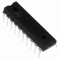
E-L4981A STMicroelectronics, E-L4981A Datasheet

E-L4981A
Specifications of E-L4981A
Available stocks
Related parts for E-L4981A
E-L4981A Summary of contents
Page 1
... PRECISE 2% ON CHIP REFERENCE EX- TERNALLY AVAILABLE SOFT START DESCRIPTION The L4981 I.C. provides the necessary features to achieve a very high power factor up to 0.99. Realized in BCD 60II technology this power factor corrector (PFC) pre-regulator contains all the con- BLOCK DIAGRAM November 2001 ...
Page 2
... Maximum package power dissipation limits must be observed. PIN CONNECTIONS (Top views) L4981A 2/16 soft start are included. To limit the number of the external components, the device integrates pro- tections as overvoltage and overcurrent. The overcurrent level can be programmed using a simple resistor for L4981A. For a better precision and for L4981B an external divider must be used ...
Page 3
... Connecting a low pass filter between the rectified line and the pin voltage proportional to the input line RMS voltage is obtained. The best control is reached using input voltage between 1.5V and 5.5V. If this function is not used connect this pin to the voltage reference (pin = 11). ...
Page 4
... L4981A - L4981B ELECTRICAL CHARACTERISTICS (Unless otherwise specified 24K , OSC SS CA-OUT V = GND 1V, V FEED IPK OVP Symbol Prameter ERROR AMPLIFIER SECTION V Input Offset Voltage IO I Input Bias Current IB Open Loop Gain V Output High voltage 13H V Output Low Voltage 13L -I Output Source Current ...
Page 5
... UNDER VOLTAGE LOCKOUT SECTION V Turn on Threshold Turn off Threshold th OFF Programmable Turn-on Threshold LOAD FEED FORWARD I Bias Current LFF V Input Voltage Range I (*) Maximum package power dissipation limits must be observed. Test Condition +100mV OVP thr -0.2V OCP thr V = -0.1V only for L4981A ...
Page 6
... A OSC 4V, V VA-OUT RMS MULTOUT LFF I = 200 A, C OSC 2V, V VA-OUT RMS MULTOUT LFF OSC AC 1.28 0.8 V 1.28 LFF 2 V VRMS V 1.28 OUT VRMS Figure 2: MULTI-OUT vs 1.7V; RMS Min. Typ 2V, 100 135 = 4V, 2 5 5.1V ...
Page 7
... Figure 3: MULTI-OUT vs 5.1V) LFFD Figure 5: MULTI-OUT vs 2.5V) LFFD Figure 7: MULTI-OUT vs 2.5V) LFFD (V = 4.4V; Figure 4: MULTI-OUT vs. I RMS (V = 1.7V; Figure 6: MULTI-OUT vs. I RMS (V = 4.4V; Figure 8: MULTI-OUT vs. I RMS L4981A - L4981B (V = 5.3V; AC RMS V = 5.1V) LFFD (V = 2.2V; AC RMS V = 2.5V) LFFD (V = 5.3V; AC RMS V = 2.5V) LFFD ...
Page 8
... FUSE BRIDGE BY214 220nF Vi 400V 88V AC to 254V AC R11 NTC 560 1% R21 5. 80kHz 200W OUT Figure 9B: L4981B Power Factor Corrector (200W) R17 806K 1% R17 806K 1% R22 1.1M FUSE BRIDGE BY214 220nF Vi 400V 88V AC to 254V AC R11 NTC 560 1% R21 5.1K ...
Page 9
... Figure 10: Reference Voltage vs. Source Refer- ence Current Figure 12: Reference Voltage vs. Junction Tem- perature Figure 14: Gate Driver Rise and Fall Time L4981A - L4981B Figure 11: Reference Voltage vs. Supply Voltage Figure 13: Switching Frequency vs. Junction Temperature Figure 15: Operating Supply Current vs. Supply Voltage 9/16 ...
Page 10
... L4981A - L4981B Figure 16: Programmable Under Voltage Lock- out Thresholds R23 (Kohm) Table 1: Programmable Under Voltage Lockout Thresholds 11V 12V 13V 14V 14.5V 15V Figure 18: Oscillator Diagram 10/16 Figure 17: Modulation Frequency Normalized 0.8 R22 = R23 6.8 0.4 0 OFF 10V 10.1V 10.5V 10.8V 10 ...
Page 11
... Figure 19: Demo Board Circuit (V BRIDGE T15A250V 88 to 264 Vac Cf .22uF 600V RAux1 ** RAux2 Figure 20: Component Layout (Dimensions 88 x 150mm). = 400V 360W R14 68 B2= D1+D2 Dz1 +D8+D9 18V L1=0.5mE42*21* gap=1.9 58/6 turns 330n 1.2M R11 R6 20*.2mm 56k 500k C3 R5 R12 C11 ...
Page 12
... L4981A - L4981B Figure 20: P.C.B. Component Side (Dimensions 88 x 150mm). Figure 20: P.C.B. Solder Side (Dimensions 88 x 150mm). 12/16 ...
Page 13
... Table 3. Nominal Power range at 220Vac mains out 176Vac 378W 220Vac 381W 264Vac 381W REFERENCE: AN628 - DESIGNING A HIGH POWER FACTOR SWITCHING PREREGULATOR WITH THE L4981 CONTINUOUS MODE V P out in 404Vdc 397W 406Vdc 395W 407Vdc 394W V P out in 410Vdc ...
Page 14
... E 7.4 7.6 0.291 e 1. 10.65 0.394 h 0.25 0.75 0.010 L 0.4 1.27 0.016 K 0˚ (min.)8˚ (max 14/16 inch MIN. TYP. MAX. 0.104 0.012 0.020 0.013 0.512 0.299 0.050 0.419 0.030 0.050 OUTLINE AND MECHANICAL DATA SO20 45˚ SO20MEC ...
Page 15
... MIN. TYP. MAX. MIN. a1 0.254 0.010 B 1.39 1.65 0.055 b 0.45 b1 0.25 D 25.4 E 8.5 e 2.54 e3 22.86 F 7.1 I 3.93 L 3.3 Z 1.34 inch MECHANICAL DATA TYP. MAX. 0.065 0.018 0.010 1.000 0.335 0.100 0.900 0.280 0.155 0.130 0.053 L4981A - L4981B OUTLINE AND DIP20 15/16 ...
Page 16
... STMicroelectronics. © 2001 STMicroelectronics – Printed in Italy – All Rights Reserved Australia - Brazil - Canada - China - Finland - France - Germany - Hong Kong - India - Israel - Italy - Japan - Malaysia - Malta - Morocco - Singapore - Spain - Sweden - Switzerland - United Kingdom - United States. ...


