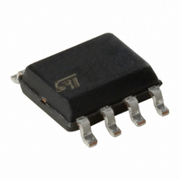
E-L6562D STMicroelectronics, E-L6562D Datasheet

E-L6562D
Specifications of E-L6562D
Available stocks
Related parts for E-L6562D
E-L6562D Summary of contents
Page 1
... Figure 1. Packages Table 1. Order Codes – HI-END AC-DC ADAPTER/CHARGER – ENTRY LEVEL SERVER & WEB SERVER 2 ® The L6562 is a current-mode PFC controller oper- ating in Transition Mode (TM). Pin-to-pin compati- ble with the predecessor L6561, it offers improved performance. COMP MULT MULTIPLIER AND ...
Page 2
... An effective two-step OVP enables to safely handle overvoltages either occurring at start-up or resulting from load disconnection. The totem-pole output stage, capable of 600 mA source and 800 mA sink current, is suitable for big MOS- FET or IGBT drive which, combined with the other features, makes the device an excellent low-cost solu- tion for EN61000-3-2 compliant SMPS 300W ...
Page 3
... Gate driver output. The totem pole output stage is able to drive power MOSFET’s and IGBT’s with a peak current of 600 mA source and 800 mA sink. The high-level voltage of this pin is clamped at about 12V to avoid excessive gate voltages in case the pin is supplied with a high Vcc ...
Page 4
... Voltage Rise Time r V Output clamp voltage Oclamp UVLO saturation (1) All parameters are in tracking (2) The multiplier output is given by: V (3) Parameters guaranteed by design, functionality tested in production. 4/ nF; unless otherwise specified) O Test Condition Open loop 2.4 V COMP INV 2.6 V COMP ...
Page 5
... Typical Electrical Characteristics Figure 4. Supply current vs. Supply voltage I CC (mA 0.5 0.1 0.05 0.01 0.005 cc(V) Figure 5. Start-up & UVLO vs. T 12.5 V CC-ON (V) 12 11 CC-OFF 9.5 ( (°C) Figure 6. IC consumption vs. T Icc [mA 1nF kHz 0. 25° Figure 7. Vcc Zener voltage vs. T ...
Page 6
... Figure 8. Feedback reference vs REF 2.6 (V) 2.55 2.5 2.45 2.4 - (°C) Figure 9. OVP current vs OVP 41 (µA) 40.5 40 39 (°C) Figure 10. E/A output clamp levels vs. T Vpin2 6 (V) Upper clamp Lower clamp 2 - (°C) 6/16 Figure 11. Delay-to-output vs D(H-L) 500 (ns) Vcc = 12 V 400 300 200 100 100 150 Figure 12 ...
Page 7
... Vcc = 12 V 140 130 120 110 100 - (°C) Figure 16. ZCD clamp levels vs ZCD (°C) Figure 17. ZCD source capability vs ZCDsrc (mA) 100 150 Figure 18. Gate-drive output low saturation j V pin7 100 150 Figure 19. Gate-drive output high saturation j V -1.5 Upper clamp Vcc - 2.0 Vcc = ± ...
Page 8
... INV will be 2.5V, then: If the output voltage experiences an abrupt change ∆Vo > 0 due to a load drop, the voltage at pin INV will be kept at 2.5V by the local feedback of the error amplifier, a network connected between pins INV and COMP that introduces a long time constant to achieve high PF (this is why ∆ ...
Page 9
... When the load of a PFC pre-regulator is very low, the output voltage tends to stay steadily above the nom- inal value, which cannot be handled by the Dynamic OVP. If this occurs, however, the error amplifier out- put will saturate low; hence, when this is detected, the external power transistor is switched off and the IC put in an idle state (Static OVP) ...
Page 10
... To maximally benefit from the THD optimizer circuit, the high-frequency filter capacitor after the bridge rec- tifier should be minimized, compatibly with EMI filtering needs. A large capacitance, in fact, introduces a conduction dead-angle of the AC input current in itself - even with an ideal energy transfer by the PFC pre- regulator - thus making the action of the optimizer circuit little effective. ...
Page 11
... Figure 25. EVAL6562-80W: PCB and component layout (Top view, real size 108 mm) Table 6. EVAL6562N: Evaluation results at full load Vin (V ) Pin ( 86.4 110 84.6 135 83.8 175 83.2 220 82.9 265 82.7 Note: measurements done with the line filter shown in figure 23 Table 7. EVAL6562N: Evaluation results at half load ...
Page 12
... L6562 Table 8. EVAL6562N: No-load measurements Vin (V ) Pin ( 110 135 (*) 175 (*) 220 (*) 265 (*) Vcc = 12V supplied externally Figure 26. Line filter (not tested for EMI compliance) used for EVAL6562N evaluation to the AC source 12/ 0.4 396.77 0.3 396.82 0.3 396.83 0.4 396.90 0.4 396.95 0.5 396 ...
Page 13
... In order to meet environmental requirements, ST offers these devices in ECOPACK packages have a Lead-free second level interconnect. The category of second Level Interconnect is marked on the package and on the inner box label, in compliance with JEDEC Standard JESD97. The maximum ratings related to soldering conditions are also marked on the inner box label. ECOPACK trademark ...
Page 14
... H 5.80 h 0.25 L 0.40 k 0˚ (min.), 8˚ (max.) ddd Note: (1) Dimensions D does not include mold flash, protru- sions or gate burrs. Mold flash, potrusions or gate burrs shall not exceed 0.15mm (.006inch) in total (both side). 14/16 inch MAX. MIN. TYP. MAX. 1.75 ...
Page 15
... May 2005 November 2005 5 First Issue 6 Modified the Style-look in compliance with the “Corporate Technical Publications Design Guide”. Changed input of the power amplifier connected to Multiplier (Fig. 2). 7 Modified Table 2: Absolute Maximim Ratings. 8 Added in Section 5 the ECOPACK Description of Changes ® certicate of conformity. ...
Page 16
... STMicroelectronics. The ST logo is a registered trademark of STMicroelectronics. Australia - Belgium - Brazil - Canada - China - Czech Republic - Finland - France - Germany - Hong Kong - India - Israel - Italy - Japan - Malaysia - Malta - Morocco - Singapore - Spain - Sweden - Switzerland - United Kingdom - United States of America ...


