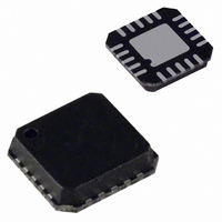
ADP5020ACPZ-R7 Analog Devices Inc, ADP5020ACPZ-R7 Datasheet - Page 11

ADP5020ACPZ-R7
Manufacturer Part Number
ADP5020ACPZ-R7
Description
IC REG LDO DUAL BUCK 20LFCSP
Manufacturer
Analog Devices Inc
Datasheet
1.ADP5020ACPZ-R7.pdf
(28 pages)
Specifications of ADP5020ACPZ-R7
Design Resources
Powering AD9272 with ADP5020 Switching Regulator PMU for Increased Efficiency (CN0135)
Applications
Handheld/Mobile Devices
Current - Supply
10mA
Voltage - Supply
2.4 V ~ 5.5 V
Operating Temperature
-40°C ~ 85°C
Mounting Type
Surface Mount
Package / Case
20-LFCSP
Supply Voltage
5.5V
No. Of Step-down Dc - Dc Converters
2
No. Of Ldo Regulators
1
Digital Ic Case Style
LFCSP
No. Of Pins
20
No. Of Regulated Outputs
3
Operating Temperature Range
-40°C To
Lead Free Status / RoHS Status
Lead free / RoHS Compliant
Other names
ADP5020ACPZ-R7TR
V
IN
= 4.5 V, V
0.90
0.85
0.80
0.75
0.70
0.65
0.60
0.55
0.50
1.2
1.0
0.8
0.6
0.4
0.2
0
2.0
BUCK 2
0
I
LOAD
Figure 14. Shutdown Current vs. Input Voltage
Figure 12. Buck 2 Efficiency vs. Load Current
OUT1
Figure 13. Buck 2 Load Transient Response
2.5
50
= 2.8 V, V
I
I
I
SHTDN
SHTDN
SHTDN
100
3.0
LOAD CURRENT (mA)
INPUT VOLTAGE (V)
OUT2
(µA) @ –40°C
(µA) @ +25°C
(µA) @ +125°C
BUCK 2 OUTPUT = 50mV/DIV
I
TIME = 100µs/DIV
LOAD
150
3.5
= V
= 100mA/DIV
OUT3
4.0
200
= 1.8 V, I
EFF1 (1.1V)
EFF2 (1.2V)
EFF3 (1.3V)
EFF4 (1.4V)
EFF5 (1.5V)
EFF6 (1.6V)
EFF7 (1.7V)
EFF8 (1.8V)
4.5
250
OUT
= 100 mA, C
5.0
300
Rev. 0 | Page 11 of 28
4
= C
1
= 10 μF, C
Figure 15. Startup Sequence of the Three Regulators, Set by Default
ENABLE
2
BUCK 2
BUCK 2
BUCK 1
= 4.7 μF, C
SW2
SW1
Figure 16. Buck 2 Enable Startup
Figure 17. Buck 1 Enable Startup
3
= 1 μF, T
J
= 25°C, unless otherwise noted.
BUCK 1 OUTPUT = 2V/DIV
BUCK 2 OUTPUT = 1V/DIV
TIME = 5ms/DIV
BUCK 2 OUTPUT = 1V/DIV
SW2 OUTPUT = 2V/DIV
TIME = 500µs/DIV
BUCK 1 OUTPUT = 1V/DIV
SW1 OUTPUT = 2V/DIV
TIME = 500µs/DIV
ADP5020


