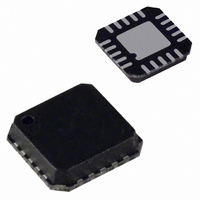
ADP5020ACPZ-R7 Analog Devices Inc, ADP5020ACPZ-R7 Datasheet - Page 17

ADP5020ACPZ-R7
Manufacturer Part Number
ADP5020ACPZ-R7
Description
IC REG LDO DUAL BUCK 20LFCSP
Manufacturer
Analog Devices Inc
Datasheet
1.ADP5020ACPZ-R7.pdf
(28 pages)
Specifications of ADP5020ACPZ-R7
Design Resources
Powering AD9272 with ADP5020 Switching Regulator PMU for Increased Efficiency (CN0135)
Applications
Handheld/Mobile Devices
Current - Supply
10mA
Voltage - Supply
2.4 V ~ 5.5 V
Operating Temperature
-40°C ~ 85°C
Mounting Type
Surface Mount
Package / Case
20-LFCSP
Supply Voltage
5.5V
No. Of Step-down Dc - Dc Converters
2
No. Of Ldo Regulators
1
Digital Ic Case Style
LFCSP
No. Of Pins
20
No. Of Regulated Outputs
3
Operating Temperature Range
-40°C To
Lead Free Status / RoHS Status
Lead free / RoHS Compliant
Other names
ADP5020ACPZ-R7TR
POWER-UP/POWER-DOWN SEQUENCE
SEQUENCER
The sequencer is enabled after a low-to-high transition of the
enable pin (EN). When EN is low or programmed as an output, the
sequencing is controlled and timed by the application processor
via the I
Each regulator inside the ADP5020 is controlled by the
sequencer block. The sequencer is factory programmed with
a default turn-on sequence that determines the activation order of
the regulators. The default activation order is listed as follows:
1.
2.
3.
A low-to-high transition of the EN pin, when programmed
as an input, or an I
REG_CONTROL_STATUS register (Address 0x03), starts the
sequencer.
The activation delay for the first regulator is determined by the
turn-on delay of the band gap, oscillator, and other internal
circuits. Therefore, the first regulator cannot be activated before
a typical 5 ms delay time has elapsed. Delays between the first
and second regulator and from the second to third regulator are
hard coded to a specific time (t
time starts from the moment a regulator has reached the power
good threshold (see Figure 22).
Buck 1
LDO
Buck 2
2
C commands.
2
C command setting Bit 4 (EN_ALL) in the
XSHTDN
BUCK 1
BUCK 2
REG1
LDO
EN
, t
REG2
, and t
Figure 22. Automatic Sequencing with EN Low-to-High Transition
t
REG1
REG3
). The delay
t
REG2
POK
Rev. 0 | Page 17 of 28
t
REG3
POK
DEFAULT POWER-ON SEQUENCE WITH EN PIN
Figure 22 shows the default regulator sequencing after a low-to-
high transition of the EN pin. The regulator order is factory
programmed and can be changed for specific applications. The
power good signal (POK) turns to high if the regulator voltage
is ≥80% of the target voltage. The second regulator checks the
POK signal of the first regulator and waits the preset delay time
(t
order, it is also possible to disable the unused regulator. Additional
fuses allow disabling of the association between XSHTDN genera-
tion and the POK signal for a specific regulator. The power good
signal of an unused regulator must be masked, via dedicated fuse
and user registers, to prevent the XSHTDN output from being
forced low. A host processor controller, connected to the I
can override the masking fuses by accessing the following bits in
the OPERATIONAL_CONTROL register (Address 0x04): Bit 3
(BK1_XSHTDN, for Buck 1), Bit 2 (BK2_XSHTDN, for Buck 2),
and Bit 3 (LDO_XSHTDN, for LDO). Writing 0 to these register
bits requires that power good be true to release the XSHTDN pin
to high. Writing 1 to these bits causes the regu-lator state to be
ignored, and XSHTDN must depend on the active and
unmasked regulators.
The regulators can also be activated individually via the I
commands. The host specifies which regulator is to be turned
on or off by setting or clearing the following selection bits in the
REG_CONTROL_STATUS register (Address 0x03): Bit 7
(BK1_EN), Bit 6 (BK2_EN), or Bit 5 (LDO_EN). When the
regulators are individually activated by I
sequencing is disabled and the host controls the turn-on and
turn-off timing (see Figure 26).
REG2
) before turning on. In addition to changing the regulator
POK
t
XSHTDN
2
C commands, the auto
ADP5020
2
2
C
C bus,


