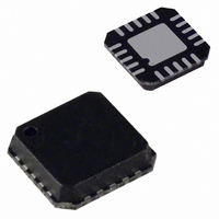
ADP5020ACPZ-R7 Analog Devices Inc, ADP5020ACPZ-R7 Datasheet - Page 7

ADP5020ACPZ-R7
Manufacturer Part Number
ADP5020ACPZ-R7
Description
IC REG LDO DUAL BUCK 20LFCSP
Manufacturer
Analog Devices Inc
Datasheet
1.ADP5020ACPZ-R7.pdf
(28 pages)
Specifications of ADP5020ACPZ-R7
Design Resources
Powering AD9272 with ADP5020 Switching Regulator PMU for Increased Efficiency (CN0135)
Applications
Handheld/Mobile Devices
Current - Supply
10mA
Voltage - Supply
2.4 V ~ 5.5 V
Operating Temperature
-40°C ~ 85°C
Mounting Type
Surface Mount
Package / Case
20-LFCSP
Supply Voltage
5.5V
No. Of Step-down Dc - Dc Converters
2
No. Of Ldo Regulators
1
Digital Ic Case Style
LFCSP
No. Of Pins
20
No. Of Regulated Outputs
3
Operating Temperature Range
-40°C To
Lead Free Status / RoHS Status
Lead free / RoHS Compliant
Other names
ADP5020ACPZ-R7TR
I
Table 6.
Parameter
f
t
t
t
t
t
t
t
t
t
t
t
C
1
2
Timing Diagram
SCL
2
HIGH
LOW
SU,DAT
HD,DAT
SU,STA
HD,STA
BUF
SU,STO
RISE
FALL
SP
A master device must provide a hold time of at least 300 ns for the SDA signal (referred to the V
C
B
C TIMING SPECIFICATIONS
2
B
is the total capacitance of one bus line in picofarads (pF).
1
SDA
S = START CONDITION
Sr = START REPEATED CONDITION
P = STOP CONDITION
SCL
Min
0.6
1.3
100
0
0.6
0.6
1.3
0.6
20 + 0.1C
20 + 0.1C
0
S
B
B
t
LOW
Max
400
0.9
300
300
50
400
t
HD,DAT
t
RISE
Unit
kHz
μs
μs
ns
μs
μs
μs
μs
μs
ns
ns
ns
pF
t
SU,DAT
Figure 3. I
Description
SCL clock frequency
SCL high time
SCL low time
Data setup time
Data hold time
Setup time for repeated start
Hold time for start/repeated start
Bus free time between a stop condition and a start condition
Setup time for stop condition
Rise time of SCL/SDA
Fall time of SCL/SDA
Pulse width of suppressed spike
Capacitive load for each bus line
t
HIGH
2
Rev. 0 | Page 7 of 28
C Interface Timing Diagram
t
t
SU,STA
FALL
Sr
IHMIN
of the SCL signal) to bridge the undefined region of the SCL falling edge.
t
FALL
t
HD,STA
t
t
SP
SU,STO
t
RISE
P
t
BUF
S
ADP5020


