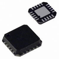
ADP5020ACPZ-R7 Analog Devices Inc, ADP5020ACPZ-R7 Datasheet - Page 8

ADP5020ACPZ-R7
Manufacturer Part Number
ADP5020ACPZ-R7
Description
IC REG LDO DUAL BUCK 20LFCSP
Manufacturer
Analog Devices Inc
Datasheet
1.ADP5020ACPZ-R7.pdf
(28 pages)
Specifications of ADP5020ACPZ-R7
Design Resources
Powering AD9272 with ADP5020 Switching Regulator PMU for Increased Efficiency (CN0135)
Applications
Handheld/Mobile Devices
Current - Supply
10mA
Voltage - Supply
2.4 V ~ 5.5 V
Operating Temperature
-40°C ~ 85°C
Mounting Type
Surface Mount
Package / Case
20-LFCSP
Supply Voltage
5.5V
No. Of Step-down Dc - Dc Converters
2
No. Of Ldo Regulators
1
Digital Ic Case Style
LFCSP
No. Of Pins
20
No. Of Regulated Outputs
3
Operating Temperature Range
-40°C To
Lead Free Status / RoHS Status
Lead free / RoHS Compliant
Other names
ADP5020ACPZ-R7TR
ADP5020
ABSOLUTE MAXIMUM RATINGS
Table 7.
Parameter
VDD1, VDD2, VDD3
SW1, SW2
VOUT1, VOUT2, VOUT3
VDD_IO
EN, SCL, SDA, SYNC, XSHTDN
Operating Temperature Range
Storage Temperature Range
Lead Temperature
V
Stresses above those listed under Absolute Maximum Ratings
may cause permanent damage to the device. This is a stress
rating only; functional operation of the device at these or any
other conditions above those indicated in the operational
section of this specification is not implied. Exposure to absolute
maximum rating conditions for extended periods may affect
device reliability.
The ADP5020 can be damaged when the junction temperature
(T
does not guarantee that T
limits. In applications with high power dissipation and poor
thermal resistance, the maximum ambient temperature may
have to be derated. In applications having moderate power dis-
sipation and low PCB thermal resistance, the maximum ambient
temperature can exceed the maximum limit as long as the junction
temperature is within specification limits. The T
dependent on the ambient temperature (T
(PD) of the device, and the junction-to-ambient thermal resistance
of the package (θ
using the following formula:
ESD
Ambient
Junction
Soldering (10 sec)
Vapor Phase (60 sec)
Infrared (15 sec)
Machine Model Range
Human Body Model Range
Charged Device Model
J
) limits are exceeded. Monitoring the ambient temperature
T
J
= T
A
+ (PD × θ
JA
). Maximum T
JA
)
J
is within the specified temperature
J
is calculated from T
Rating
−0.3 V to +6 V
−0.3 V to +6 V
−0.3 V to +6 V
−0.3V to +3.6 V
−0.3 V to V
−40°C to +85°C
−40°C to +125°C
−65°C to +150°C
260°C
260°C
215°C
220°C
−200 V to +200 V
−2000 V to +2000 V
±750 V
A
), the power dissipation
J
of the device is
DD_IO
A
+ 0.3 V
and PD
Rev. 0 | Page 8 of 28
THERMAL RESISTANCE
θ
soldered in a circuit board for surface-mount packages.
Table 8. Thermal Resistance
Package Type
20-Lead LFCSP (CP-20-4)
Thermal Data
Junction-to-ambient thermal resistance (θ
based on modeling and calculation using a 4-layer board. The
junction-to-ambient thermal resistance is highly dependent on
the application and board layout. In applications where high maxi-
mum power dissipation exists, attention to thermal board design
is required. The value of θ
layout, and environmental conditions. The specified value of θ
is based on a 4-layer, 4 in × 3 in, 2 1/2 oz copper board, as per
JEDEC standards. For more information, see the AN-772
Application Note, A Design and Manufacturing Guide for the
Lead Frame Chip Scale Package (LFCSP).
ESD CAUTION
JA
is specified for the worst-case conditions, that is, a device
JA
may vary, depending on PCB material,
θ
47.4
JA
JA
θ
4.3
) of the package is
JC
Unit
°C/W
JA


