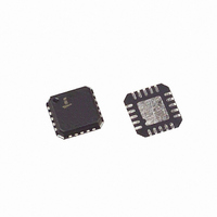
ISL6532CRZ Intersil, ISL6532CRZ Datasheet - Page 10

ISL6532CRZ
Manufacturer Part Number
ISL6532CRZ
Description
IC CTRLR PWM 2CHAN DDR 20QFN
Manufacturer
Intersil
Datasheet
1.ISL6532CRZ.pdf
(14 pages)
Specifications of ISL6532CRZ
Applications
Memory, DDR/DDR2 Regulator
Current - Supply
5.25mA
Operating Temperature
0°C ~ 70°C
Mounting Type
Surface Mount
Package / Case
20-QFN
Lead Free Status / RoHS Status
Lead free / RoHS Compliant
Voltage - Supply
-
Available stocks
Company
Part Number
Manufacturer
Quantity
Price
Part Number:
ISL6532CRZ
Manufacturer:
INTERSIL
Quantity:
20 000
represent numerous physical capacitors. Dedicate one solid
layer, usually a middle layer of the PC board, for a ground
plane and make all critical component ground connections
with vias to this layer. Dedicate another solid layer as a
power plane and break this plane into smaller islands of
common voltage levels. Keep the metal runs from the
PHASE terminals to the output inductor short. The power
plane should support the input power and output power
nodes. Use copper filled polygons on the top and bottom
circuit layers for the phase nodes. Use the remaining printed
circuit layers for small signal wiring. The wiring traces from
the GATE pins to the MOSFET gates should be kept short
and wide enough to easily handle the 1A of drive current.
In order to dissipate heat generated by the internal V
the ground pad, pin 21, should be connected to the internal
ground plane through at least four vias. This allows the heat
to move away from the IC and also ties the pad to the ground
plane through a low impedance path.
FIGURE 4. PRINTED CIRCUIT BOARD POWER PLANES
12V
KEY
ATX
ISL6532
GND PAD
VIA CONNECTION TO GROUND PLANE
ISLAND ON POWER PLANE LAYER
ISLAND ON CIRCUIT PLANE LAYER
P12V
VDDQ(2)
P5VSBY
5VSBY
LGATE
UGATE
AND ISLANDS
VTT(2)
COMP
GND
NCH
GND
FB
C
C
BP
OUT2
R
C
C
2
2
BP
5VSBY
R
10
4
C
1
C
3
R
V
V
Q
1
Q
DDQ
TT
R
1
V
2
3
IN_DDR
L
OUT
C
C
IN
OUT1
V
DDQ
TT
LDO,
ISL6532
The switching components should be placed close to the
ISL6532 first. Minimize the length of the connections
between the input capacitors, C
by placing them nearby. Position both the ceramic and bulk
input capacitors as close to the upper MOSFET drain as
possible. Position the output inductor and output capacitors
between the upper and lower MOSFETs and the load.
The critical small signal components include any bypass
capacitors, feedback components, and compensation
components. Place the PWM converter compensation
components close to the FB and COMP pins. The feedback
resistors should be located as close as possible to the FB
pin with vias tied straight to the ground plane as required.
Feedback Compensation - PWM Buck Converter
Figure 5 highlights the voltage-mode control loop for a
synchronous-rectified buck converter. The output voltage
(V
error amplifier output (V
(OSC) triangular wave to provide a pulse-width modulated
(PWM) wave with an amplitude of V
The PWM wave is smoothed by the output filter (L
The modulator transfer function is the small-signal transfer
function of V
Gain and the output filter (L
break frequency at F
V
∆V
DDQ
OUT
OSC
FIGURE 5. VOLTAGE-MODE BUCK CONVERTER
) is regulated to the Reference voltage level. The
=
OSC
0.8
×
OUT
COMPARATOR
COMPENSATION DESIGN AND OUTPUT
VOLTAGE SELECTION
ERROR
AMP
DETAILED COMPENSATION COMPONENTS
V
1
ISL6532
E/A
+
PWM
/V
R
------ -
R
E/A
Z
+
-
1
4
FB
-
+
COMP
LC
C
. This function is dominated by a DC
REFERENCE
2
REFERENCE
and a zero at F
E/A
C
+
-
1
O
) is compared with the oscillator
DRIVER
DRIVER
R
and C
Z
2
IN
IN
, and the power switches
FB
O
Z
IN
FB
), with a double pole
ESR
PHASE
at the PHASE node.
R
(PARASITIC)
V
4
C
IN
3
L
Z
R
. The DC Gain of
O
IN
1
R
ESR
C
3
O
O
V
DDQ
and C
V
DDQ
O
).


