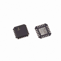
ISL6532CRZ Intersil, ISL6532CRZ Datasheet - Page 7

ISL6532CRZ
Manufacturer Part Number
ISL6532CRZ
Description
IC CTRLR PWM 2CHAN DDR 20QFN
Manufacturer
Intersil
Datasheet
1.ISL6532CRZ.pdf
(14 pages)
Specifications of ISL6532CRZ
Applications
Memory, DDR/DDR2 Regulator
Current - Supply
5.25mA
Operating Temperature
0°C ~ 70°C
Mounting Type
Surface Mount
Package / Case
20-QFN
Lead Free Status / RoHS Status
Lead free / RoHS Compliant
Voltage - Supply
-
Available stocks
Company
Part Number
Manufacturer
Quantity
Price
Part Number:
ISL6532CRZ
Manufacturer:
INTERSIL
Quantity:
20 000
FB (Pin 11) and COMP (Pin 12)
The V
control loop. FB is the negative input to the voltage loop error
amplifier. The positive input of the error amplifier is
connected to a precision 0.8V reference and the output of
the error amplifier is connected to the COMP pin. The V
output voltage is set by an external resistor divider
connected to FB. With a properly selected divider, V
be set to any voltage between the power rail (reduced by
converter losses) and the 0.8V reference. Loop
compensation is achieved by connecting an AC network
across COMP and FB.
The FB pin is also monitored for under and over-voltage
events.
VDDQ (Pins 5, 6)
The V
the regulated V
pins serve as inputs to the V
Reference precision divider. During S3 (Suspend to RAM)
state, the V
standby LDO.
VTT (Pins 3, 4)
The VTT pins should be connected together. During S0/S1
states, the VTT pins serve as the outputs of the V
regulator. During any sleep state, the V
disabled.
VTTSNS (Pin 7)
VTTSNS is used as the feedback for control of the V
regulator. Connect this pin to the V
point of desired regulation.
VREF_OUT (Pin 9)
VREF_OUT is a buffered version of V
reference voltage for the V
recommended that a minimum capacitance of 0.1µF be
connected between V
between VREF_OUT and GND for proper operation.
VREF_IN (Pin 10)
A capacitor, C
is required. This capacitor and the parallel combination of
the Upper and Lower Divider Impedance (R
time constant for the start up ramp when transitioning from
S3 to S0/S1/S2.
The minimum value for C
following equation:
The calculated capacitance, C
capacitor bank on the V
reaching the current limit of the V
C
SS
>
DDQ
DDQ
C
------------------------------------------------
10 2A R
VTTOUT
⋅
switching regulator employs a single voltage
pins should be connected externally together to
DDQ
SS
⋅
DDQ
⋅
pins serve as an output from the integrated
, connected between VREF_IN and ground
U
V
||
DDQ
R
output. During S0/S1 states, the V
L
DDQ
TT
SS
TT
rail in a controlled manner without
and VREF_OUT and also
TT
can be found through the
linear regulator. It is
7
SS
regulator and to the V
, will charge the output
TT
TT
LDO.
TT
output at the physical
TT
and also acts as the
regulator is
U
||R
L
), sets the
TT
DDQ
TT
linear
TT
linear
DDQ
DDQ
can
ISL6532
NCH (Pin 15)
NCH is an open-drain output that controls the MOSFET
blocking backfeed from V
states. A 2kΩ or larger resistor is to be tied between the 12V
rail and the NCH pin. Until the voltage on the NCH pin
reaches the NCH trip level, the PWM is disabled.
If NCH is not actively utilized, it still must be tied to the 12V
rail through a resistor. For systems using 5V dual as the
input to the switching regulator, a time constant, in the form
of a capacitor, can be added to the NCH pad to delay start of
the PWM switcher until the 5V dual has switched from
5VSBY to 5VATX.
PGOOD (Power Good) (Pin 14)
Power Good is an open-drain logic output that changes to a
logic low if the V
state. PGOOD will always be low in any state other than
S0/S1/S2.
S5# (Pin 17)
This pin accepts the SLP_S5# sleep state signal.
S3# (Pin 16)
This pin accepts the SLP_S3# sleep state signal.
Functional Description
Overview
The ISL6532 provides complete control, drive, protection
and ACPI compliance for a regulator powering DDR memory
systems. It is primarily designed for computer applications
powered from an ATX power supply. A 250kHz Synchronous
Buck Regulator with a precision 0.8V reference provides the
proper Core voltage to the system memory of the computer.
An internal LDO regulator with the ability to both sink and
source current and an externally available buffered reference
that tracks the V
termination voltage.
ACPI compliance is realized through the SLP_S3 and
SLP_S5 sleep signals and through monitoring of the 12V
ATX bus.
Initialization
The ISL6532 automatically initializes upon receipt of input
power. Special sequencing of the input supplies is not
necessary. The Power-On Reset (POR) function continually
monitors the input bias supply voltages. The POR monitors
the bias voltage at the 5VSBY and P12V pins. The POR
function initiates soft-start operation after the bias supply
voltages exceed their POR thresholds.
ACPI State Transitions
Cold Start (S5/S4 to S0 Transition)
At the onset of a mechanical start, the ISL6532 receives it’s
bias voltage from the 5V Standby bus (5VSBY). As soon as
the SLP_S3 and SLP_S5 signals have transitioned HIGH,
TT
DDQ
regulator is out of regulation in S0/S1/S2
output by 50% provides the V
DDQ
to the input rail during sleep
TT


