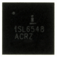
ISL6548ACRZA Intersil, ISL6548ACRZA Datasheet - Page 13

ISL6548ACRZA
Manufacturer Part Number
ISL6548ACRZA
Description
IC REG/CTLR ACPI DUAL DDR 28QFN
Manufacturer
Intersil
Datasheet
1.ISL6548ACRZA-T.pdf
(16 pages)
Specifications of ISL6548ACRZA
Applications
Memory, DDR/DDR2 Regulator
Current - Supply
7mA
Operating Temperature
0°C ~ 70°C
Mounting Type
Surface Mount
Package / Case
28-QFN
Rohs Compliant
YES
Lead Free Status / RoHS Status
Lead free / RoHS Compliant
Voltage - Supply
-
Available stocks
Company
Part Number
Manufacturer
Quantity
Price
Company:
Part Number:
ISL6548ACRZA
Manufacturer:
Intersil
Quantity:
100
Part Number:
ISL6548ACRZA
Manufacturer:
INTERSIL
Quantity:
20 000
Part Number:
ISL6548ACRZA-T
Manufacturer:
INTERSIL
Quantity:
20 000
The modulator transfer function is the small-signal transfer
function of V
Gain and the output filter (L
break frequency at F
the modulator is simply the input voltage (V
peak-to-peak oscillator voltage ∆V
Modulator Break Frequency Equations
The compensation network consists of the error amplifier
(internal to the ISL6548A) and the impedance networks Z
and Z
a closed loop transfer function with the highest 0dB crossing
frequency (f
is the difference between the closed loop phase at f
180 degrees. The equations below relate the compensation
network’s poles, zeros and gain to the components (R
R
locating the poles and zeros of the compensation network:
Compensation Break Frequency Equations
Figure 4 shows an asymptotic plot of the DC/DC converter’s
gain vs. frequency. The actual Modulator Gain has a high gain
peak due to the high Q factor of the output filter and is not
shown in Figure 4. Using the above guidelines should give a
Compensation Gain similar to the curve plotted. The open
loop error amplifier gain bounds the compensation gain.
Check the compensation gain at F
the error amplifier. The Closed Loop Gain is constructed on
the graph of Figure 4 by adding the Modulator Gain (in dB) to
the Compensation Gain (in dB). This is equivalent to
multiplying the modulator transfer function to the
compensation transfer function and plotting the gain.
The compensation gain uses external impedance networks
Z
loop. A stable control loop has a gain crossing with
-20dB/decade slope and a phase margin greater than 45
degrees. Include worst case component variations when
determining phase margin.
F LC
F
F
1. Pick Gain (R
2. Place 1
3. Place 2
4. Place 1
5. Place 2
6. Check Gain against Error Amplifier’s Open-Loop Gain.
7. Estimate Phase Margin - Repeat if Necessary.
FB
3
Z1
Z2
, C
=
and Z
=
=
FB
1
------------------------------------------ -
2π x
, C
----------------------------------- -
2π x R
------------------------------------------------------ -
2π x R
. The goal of the compensation network is to provide
2
IN
ST
, and C
ND
ST
ND
0dB
(
OUT
1
to provide a stable, high bandwidth (BW) overall
L O x C O
1
2
Zero Below Filter’s Double Pole (~75% F
1
Pole at the ESR Zero.
Zero at Filter’s Double Pole.
Pole at Half the Switching Frequency.
x C
) and adequate phase margin. Phase margin
1
+
2
/V
R
/R
1
3
3
E/A
) in Figure 3. Use these guidelines for
1
) x C
LC
) for desired converter bandwidth.
. This function is dominated by a DC
and a zero at F
3
O
13
F ESR
F
F
and C
P1
P2
P2
=
=
OSC
=
O
-------------------------------------------------------- -
2π x R
----------------------------------- -
2π x R
with the capabilities of
------------------------------------------- -
2π x ESR x C O
), with a double pole
ESR
.
1
2
3
IN
. The DC Gain of
1
x
x C
) divided by the
1
C
--------------------- -
C
3
1
1
x C
+
0dB
C
2
2
LC
1
, R
and
).
IN
2
ISL6548A
,
Output Voltage Selection
The output voltage of the all the external voltage regulators
converter can be programmed to any level between their
individual input voltage and the internal reference, 0.8V. An
external resistor divider is used to scale the output voltage
relative to the reference voltage and feed it back to the
inverting input of the error amplifier, refer to the Typical
Application on page 4.
The output voltage programming resistor will depend on the
value chosen for the feedback resistor and the desired
output voltage of the particular regulator.
If the output voltage desired is 0.8V, simply route the output
voltage back to the respective FB pin through the feedback
resistor and do not populate the output voltage programming
resistor.
The output voltage for the internal V
is set internal to the ISL6548A to track the V
50%. There is no need for external programming resistors.
R4
R8
R10
R12
FIGURE 4. ASYMPTOTIC BODE PLOT OF CONVERTER GAIN
100
-20
-40
-60
80
60
40
20
0
=
=
=
=
---------------------------------- -
V
--------------------------------------- -
V
10
---------------------------------------------------------- -
V
----------------------------------
V
(R
20LOG
R1
DDQ
GMCH
R11 0.8V
R5
xxxxxxxxxxxx
TT_GMCH/CPU
DAC
MODULATOR
2
/R
×
×
1
–
0.8V
×
GAIN
R9
)
–
0.8V
100
0.8V
–
0.8V
0.8V
×
0.8V
1K
–
F
Z1
0.8V
F
FREQUENCY (Hz)
LC
F
Z2
10K
F
F
P1
ESR
(V
100K
IN
20LOG
F
TT_DDR
/∆V
P2
OSC
OPEN LOOP
ERROR AMP GAIN
1M
)
DDQ
linear regulator
COMPENSATION
CLOSED LOOP
10M
January 3, 2006
voltage by
GAIN
GAIN
FN9189.2


