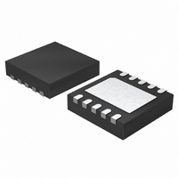
LT3485EDD-2#PBF Linear Technology, LT3485EDD-2#PBF Datasheet

LT3485EDD-2#PBF
Specifications of LT3485EDD-2#PBF
Available stocks
Related parts for LT3485EDD-2#PBF
LT3485EDD-2#PBF Summary of contents
Page 1
... The LT3485 series of parts are housed in a leadless (3mm × 3mm) DFN package. , LT, LTC and LTM are registered trademarks of Linear Technology Corporation. All other trademarks are the property of their respective owners. Protected by U.S. Patents including 6636021. ...
Page 2
... EXPOSED PAD (11) IS GND, MUST BE SOLDERED TO PCB ORDER PART NUMBER LT3485EDD-0 LT3485EDD-1 LT3485EDD-2 LT3485EDD-3 Order Options Tape and Reel: Add #TR Lead Free: Add #PBF Lead Free Tape and Reel: Add #TRPBF Lead Free Part Marking: Consult LTC Marketing for parts specified with wider operating temperature ranges. ...
Page 3
ELECTRICAL CHARACTERISTICS temperature range, otherwise specifications are at T PARAMETER Switch Leakage Current CHARGE Input Voltage High CHARGE Input Voltage Low Minimum Charge Pin Low Time DONE Output Signal High DONE Output Signal Low DONE Leakage Current IGBT Input Voltage ...
Page 4
LT3485-0/LT3485-1/ LT3485-2/LT3485 TYPICAL PERFOR A CE CHARACTERISTICS curves use the circuit of Figure 9, LT3485-2 use the circuit of Figure 10 and LT3485-3 use the circuit of Figure 11 unless otherwise noted. LT3485-0 Charging Waveform V OUT 50V/DIV ...
Page 5
W U TYPICAL PERFOR A CE CHARACTERISTICS curves use the circuit of Figure 9, LT3485-2 use the circuit of Figure 10 and LT3485-3 use the circuit of Figure 11 unless otherwise noted. LT3485-0 Efficiency 2.5V ...
Page 6
LT3485-0/LT3485-1/ LT3485-2/LT3485 TYPICAL PERFOR A CE CHARACTERISTICS curves use the circuit of Figure 9, LT3485-2 use the circuit of Figure 10 and LT3485-3 use the circuit of Figure 11 unless otherwise noted. LT3485-0 Switching Waveform V SW 10V/DIV ...
Page 7
CTIO S CHARGE (Pin 1): Charge Pin. A low (<0.3V) to high (>1V) transition on this pin puts the part into power delivery mode. Once the target voltage is reached, the part will stop charging ...
Page 8
LT3485-0/LT3485-1/ LT3485-2/LT3485 CTIO AL BLOCK DIAGRA DONE V MONT SAMPLE AND HOLD CHARGE ONE- 1 SHOT IGBT DRIVER IN POWER 7 IGBTIN IGBT ...
Page 9
U OPERATIO The LT3485-0/LT3485-1/LT3485-2/LT3485-3 are designed to charge photoflash capacitors quickly and efficiently. The operation of the part can be best understood by referring to Figure 1. When the CHARGE pin is first driven high, a one shot sets both ...
Page 10
LT3485-0/LT3485-1/ LT3485-2/LT3485 APPLICATIO S I FOR ATIO Choosing the Right Device (LT3485-0/LT3485-1/LT3485-2/LT3485-3) The only difference between the four versions of the LT3485 is the peak current level. For the fastest possible charge time, use the LT3485-3. The LT3485-1 ...
Page 11
... SW pin, the parasitic capacitance of the transformer would become large. This will adversely affect the charge time of the photoflash circuit. Linear Technology has worked with several leading mag- netic component manufacturers to produce pre-designed flyback transformers for use with the LT3485-0/LT3485- 1/LT3485-2/LT3485-3 ...
Page 12
LT3485-0/LT3485-1/ LT3485-2/LT3485 APPLICATIO S I FOR ATIO The peak current of the diode is simply LT3485-3 PK-SEC N 1 LT3485-0 PK-SEC LT3485-2 ...
Page 13
U U APPLICATIO S I FOR ATIO GATE EMITTER Figure 6. IGBT Gate the capacitance closest to the terminal goes low but the capacitance further from the terminal remains high. This causes a small portion of the device to handle ...
Page 14
LT3485-0/LT3485-1/ LT3485-2/LT3485 APPLICATIO S I FOR ATIO Board Layout The high voltage operation of the LT3485-0/LT3485-1/ LT3485-2/LT3485-3 demands careful attention to board layout. You will not get advertised performance with careless layout. Figure 7 shows the recommended com- ...
Page 15
U TYPICAL APPLICATIO 2. Figure 8. LT3485-0 Photoflash Charger Uses High Efficiency 4mm Tall Transformer Figure 9. LT3485-1 Photoflash Charger Uses High Efficiency 3mm Tall Transformer T1 1:10.2 V BAT ...
Page 16
LT3485-0/LT3485-1/ LT3485-2/LT3485-3 U TYPICAL APPLICATIO 2. Figure 10. LT3485-2 Photoflash Charger Uses High Efficiency 4mm Tall Transformer Figure 11. LT3485-3 Photoflash Charger Uses High Efficiency 3mm Tall Transformer 16 T1 ...
Page 17
U TYPICAL APPLICATIO 2. Figure 12. LT3485-0 Photoflash Circuit Uses Tiny 3mm Tall Transformer Figure 13. Charge Time with TDK Transformers (Figures 11, 12, 13, 14 and 15) T1 1:10.2 V BAT 1. ...
Page 18
LT3485-0/LT3485-1/ LT3485-2/LT3485-3 U TYPICAL APPLICATIO 2. Figure 14. LT3485-1 Photoflash Circuit Uses Tiny 3mm Tall Transformer Figure 15. LT3485-2 Photoflash Circuit Uses Tiny 3mm Tall Transformer 18 T1 1:10.2 V ...
Page 19
... SHADED AREA IS ONLY A REFERENCE FOR PIN 1 LOCATION ON THE TOP AND BOTTOM OF PACKAGE Information furnished by Linear Technology Corporation is believed to be accurate and reliable. However, no responsibility is assumed for its use. Linear Technology Corporation makes no represen- tation that the interconnection of its circuits as described herein will not infringe on existing patent rights Package 10-Lead Plastic DFN (3mm × ...
Page 20
... DC/DC Converter for CCD Bias LT3463/LT3463A Dual Boost (250mA)/Inverting (250mA/400mA) DC/DC Converter for CCD Bias LT3484-0/LT3484-1/ Photoflash Capacitor Chargers LT3484-2 ThinSOT is a trademark of Linear Technology Corporation. Linear Technology Corporation 20 1630 McCarthy Blvd., Milpitas, CA 95035-7417 (408) 432-1900 FAX: (408) 434-0507 ● ...


