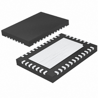
LTC3586EUFE#PBF Linear Technology, LTC3586EUFE#PBF Datasheet - Page 19

LTC3586EUFE#PBF
Manufacturer Part Number
LTC3586EUFE#PBF
Description
IC MANAGER USB PWR HI-EFF 38QFN
Manufacturer
Linear Technology
Datasheet
1.LTC3586EUFEPBF.pdf
(36 pages)
Specifications of LTC3586EUFE#PBF
Applications
Handheld/Mobile Devices
Voltage - Supply
4.35 V ~ 5.5 V
Operating Temperature
-40°C ~ 85°C
Mounting Type
Surface Mount
Package / Case
38-QFN
Lead Free Status / RoHS Status
Lead free / RoHS Compliant
Current - Supply
-
Available stocks
Company
Part Number
Manufacturer
Quantity
Price
operaTion
Thermal Regulation
To optimize charging time, an internal thermal feedback
loop may automatically decrease the programmed charge
current. This will occur if the die temperature rises to
approximately 110°C. Thermal regulation protects the
LTC3586/LTC3586-1 from excessive temperature due to
high power operation or high ambient thermal conditions
and allows the user to push the limits of the power handling
capability with a given circuit board design without risk of
damaging the LTC3586/LTC3586-1 or external components.
The benefit of the LTC3586/LTC3586-1 thermal regulation
loop is that charge current can be set according to actual
conditions rather than worst-case conditions with the as-
surance that the battery charger will automatically reduce
the current in worst-case conditions.
A flow chart of battery charger operation can be seen in
Figure 4.
Low Supply Operation
The LTC3586/LTC3586-1 incorporate an undervoltage
lockout circuit on V
purpose switching regulators when V
V
FAULT Pin
FAULT is a bi-directional pin with an open-drain output used
to indicate a fault condition on any of the general purpose
regulators. If any of the four regulators are enabled, and
their corresponding FB pin voltage does not rise to within
8% of the internal reference voltage (0.8V) within 14ms, a
fault condition will be reported by FAULT going low. This,
in turn, will disable all of the regulators. Alternatively, the
regulators can be all disabled simultaneously by driving
FAULT low externally. This fault condition can be cleared
only if all of the ENABLE inputs are pulled low for at least
3.6µs. Since FAULT is an open-drain output, it requires
a pull-up resistor to the input voltage of the monitoring
microprocessor or another appropriate power source
such as LD03V3.
If any of the ENABLE pins is tied high during start-up,
the FAULT pin can erroneously report a fault condition.
To avoid such an event, the ENABLE pins should be tied
high through a lowpass filter (comprised of a 1k resistor
OUTUVLO
. This UVLO prevents unstable operation.
OUT
which shuts down all four general
OUT
drops below
and a 0.1µF capacitor) to the same power source to which
FAULT pin is pulled up.
General Purpose Buck Switching Regulators
The LTC3586/LTC3586-1 contain two 2.25MHz constant-
frequency current mode buck switching regulators. Each
buck regulator can provide up to 400mA of output current.
Both buck regulators can be programmed for a minimum
output voltage of 0.8V and can be used to power a micro-
controller core, microcontroller I/O, memory, disk drive or
other logic circuitry. Both buck converters support 100%
duty cycle operation (low dropout mode) when their input
voltage drops very close to their output voltage. To suit a
variety of applications, selectable mode functions can be
used to trade-off noise for efficiency. Two modes are avail-
able to control the operation of the LTC3586/LTC3586-1’s
buck regulators. At moderate to heavy loads, the pulse-
skip mode provides the least noise switching solution. At
lighter loads, Burst Mode operation may be selected. The
buck regulators include soft-start to limit inrush current
when powering on, short-circuit current protection and
switch node slew limiting circuitry to reduce radiated
EMI. No external compensation components are required.
The operating mode of the buck regulators can be set by
the MODE pin. The buck converters can be individually
enabled by the EN1 and EN2 pins. Both buck regulators
have a fixed feedback servo voltage of 800mV. The buck
regulator input supplies V
connected to the system load pin V
Buck Regulator Output Voltage Programming
Both buck regulators can be programmed for output volt-
ages greater than 0.8V. The output voltage for each buck
regulator is programmed using a resistor divider from the
buck regulator output connected to the feedback pins (FB1
and FB2) such that:
where V
Typical values for R1 are in the range of 40k to 1M. The
capacitor C
V
OUTX
FB
=
FB
is fixed at 0.8V and X = 1, 2. See Figure 4.
V
FBX
cancels the pole created by feedback resistors
LTC3586/LTC3586-1
R
R
2
1
+
1
IN1
and V
OUT
IN2
.
will generally be
3586fb


