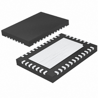
LTC3586EUFE-1#TRPBF Linear Technology, LTC3586EUFE-1#TRPBF Datasheet - Page 23

LTC3586EUFE-1#TRPBF
Manufacturer Part Number
LTC3586EUFE-1#TRPBF
Description
IC POWER MANAGER USB 38-QFN
Manufacturer
Linear Technology
Datasheet
1.LTC3586EUFEPBF.pdf
(36 pages)
Specifications of LTC3586EUFE-1#TRPBF
Applications
Handheld/Mobile Devices
Voltage - Supply
4.35 V ~ 5.5 V
Operating Temperature
-40°C ~ 85°C
Mounting Type
Surface Mount
Package / Case
38-QFN
Lead Free Status / RoHS Status
Lead free / RoHS Compliant
Current - Supply
-
Available stocks
Company
Part Number
Manufacturer
Quantity
Price
always on (and switch B always off), to step-up the input
voltage to the programmed output. If V
programmed V
4-switch mode. In this case the switches sequence through
the pattern of AD, AC, BD to either step the input voltage
up or down to the programmed output.
Buck-Boost Regulator Burst-Mode Operation
In Burst Mode operation, the buck-boost regulator uses
a hysteretic FB3 voltage algorithm to control the output
voltage. By limiting FET switching and using a hysteretic
control loop, switching losses are greatly reduced. In this
mode output current is limited to 50mA typical. While
operating in Burst Mode operation, the output capacitor
is charged to a voltage slightly higher than the regulation
point. The buck-boost converter then goes into a sleep
state, during which the output capacitor provides the load
current. The output capacitor is charged by charging the
inductor until the input current reaches 250mA typical
and then discharging the inductor until the reverse current
reaches 0mA typical. This process is repeated until the
feedback voltage has charged to 6mV above the regulation
point. In the sleep state, most of the regulator’s circuitry
is powered down, helping to conserve battery power.
When the feedback voltage drops 6mV below the regula-
tion point, the switching regulator circuitry is powered on
and another burst cycle begins. The duration for which
the regulator sleeps depends on the load current and
output capacitor value. The sleep time decreases as the
load current increases. The buck-boost regulator will not
go to sleep if the current is greater than 50mA, and if the
load current increases beyond this point while in Burst
Mode operation the output will lose regulation. Burst
Mode operation provides a significant improvement in
efficiency at light loads at the expense of higher output ripple
when compared to PWM mode. For many noise-sensitive
systems, Burst Mode operation might be undesirable at
certain times (i.e. during a transmit or receive cycle of a
wireless device), but highly desirable at others (i.e. when
the device is in low power standby mode). The MODE pin
is used to enable or disable Burst Mode operation at any
time, offering both low noise and low power operation
when they are needed.
operaTion
OUT3
, then the converter will operate in
IN3
is close to the
Buck-Boost Regulator Soft-Start Operation
Soft-start is accomplished by gradually increasing the
maximum V
Ramping the V
the V
startup. A soft-start cycle occurs whenever the buck-boost
is enabled, or after a fault condition has occurred (thermal
shutdown or UVLO). A soft-start cycle is not triggered by
changing operating modes. This allows seamless output
operation when transitioning between Burst Mode opera-
tion and PWM mode.
SYNCHRONOUS BOOST DC/DC SWITCHING
REGULATOR
The LTC3586/LTC3586-1 contain a 2.25MHz constant-
frequency current mode synchronous boost switching
regulator with true output disconnect feature. The regulator
provides at least 800mA of output load current and the
output voltage can be programmed up to a maximum of
5V. The converter is enabled by pulling EN4 high. The
boost regulator also includes soft-start to limit inrush
current and voltage overshoot when powering on, short
circuit current protection and switch node slew limiting
circuitry for reduced radiated EMI.
Error Amp
The boost output voltage is programmed by a user-sup-
plied resistive divider returned to the FB4 pin. An internally
compensated error amplifier compares the divided output
voltage with an internal 0.8V reference and adjusts the
voltage accordingly until FB4 servos to 0.8V.
Current Limit
Lossless current sensing converts the NMOS switch cur-
rent signal to a voltage to be summed with the internal
slope compensation signal. The summed signal is then
compared to the error amplifier output to provide a peak
current control command for the peak comparator. Peak
switch current is limited to 2.4A independent of output
voltage.
OUT3
voltage minimizing output overshoot during
C3
C3
voltage over a 0.5ms (typical) period.
LTC3586/LTC3586-1
voltage limits the duty cycle and thus
3586fb


