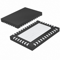
LTC3586EUFE-1#TRPBF Linear Technology, LTC3586EUFE-1#TRPBF Datasheet - Page 31

LTC3586EUFE-1#TRPBF
Manufacturer Part Number
LTC3586EUFE-1#TRPBF
Description
IC POWER MANAGER USB 38-QFN
Manufacturer
Linear Technology
Datasheet
1.LTC3586EUFEPBF.pdf
(36 pages)
Specifications of LTC3586EUFE-1#TRPBF
Applications
Handheld/Mobile Devices
Voltage - Supply
4.35 V ~ 5.5 V
Operating Temperature
-40°C ~ 85°C
Mounting Type
Surface Mount
Package / Case
38-QFN
Lead Free Status / RoHS Status
Lead free / RoHS Compliant
Current - Supply
-
Available stocks
Company
Part Number
Manufacturer
Quantity
Price
The compensation network depicted in Figure 9 yields the
transfer function:
A Type III compensation network attempts to introduce
a phase bump at a higher frequency than the LC double
pole. This allows the system to cross unity gain after the
LC double pole, and achieve a higher bandwidth. While
attempting to crossover after the LC double pole, the
system must still crossover before the boost right-half
plane zero. If unity gain is not reached sufficiently before
the right-half plane zero, then the –180° of phase from
the LC double pole combined with the –90° of phase from
the right-half plane zero will negate the phase bump of
the compensator.
The compensator zeros should be placed either before
or only slightly after the LC double pole such that their
positive phase contributions of the compensation network
offset the –180° that occurs at the filter double pole. If they
are placed at too low of a frequency, however, they will
introduce too much gain to the system and the crossover
frequency will be too high. The two high frequency poles
should be placed such that the system crosses unity gain
during the phase bump introduced by the zeros yet before
the boost right-half plane zero and such that the compen-
sator bandwidth is less than the bandwidth of the error
amp (typically 900kHz). If the gain of the compensation
network is ever greater than the gain of the error amplifier,
then the error amplifier no longer acts as an ideal op amp,
another pole will be introduced where the gain crossover
occurs, and the total compensation gain will not exceed
that of the amplifier.
applicaTions inForMaTion
V
V
OUT
C
3
3
=
•
R R
s
1
R
•
s
•
1
+
+
s
3
R
R
+
•
3
2
C
R
1
•
1
2
C
C
2
1
•
C C
+
1
•
C
•
2
s
2
+
(
•
R
1
s
+ +
+
R
1
R
3
3 3
)
•
1
• C
C
3
3
Recommended Type III Compensation Components for
a 3.3V output:
BOOST REGULATOR APPLICATIONS SECTION
Boost Regulator Inductor Selection
The boost converter is designed to work with inductors in
the range of 1µH to 5µH. For most applications a 2.2µH
inductor will suffice. Larger value inductors will allow
greater output current capability by reducing the inductor
ripple current. However, using too large an inductor may
push the right-half-plane zero too far inside and cause loop
instability. Lower value inductors result in higher ripple
current and improved transient response time. Refer to
Table 7 for recommended inductors.
Boost Regulator Input/Output Capacitor Selection
Low ESR (equivalent series resistance) ceramic capacitors
should be used at both the boost regulator output (V
as well as the boost regulator input supply (V
X5R or X7R ceramic capacitors should be used because
they retain their capacitance over wider voltage and tem-
perature ranges than other ceramic types. At least 10µF of
output capacitance at the rated output voltage is required to
ensure stability of the boost converter output voltage over
the entire temperature and load range. Refer to Table 6 for
recommended ceramic capacitor manufacturers.
R1: 324k
R
C1: 10pF
R2: 15k
C2: 330pF
R3: 121k
C3: 33pF
C
L
OUT
OUT
FB
: 105k
: 2.2µH
: 22µF
LTC3586/LTC3586-1
IN4
). Only
OUT4
3586fb
)


