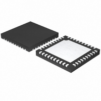
ISL97653AIRZ-TK Intersil, ISL97653AIRZ-TK Datasheet

ISL97653AIRZ-TK
Specifications of ISL97653AIRZ-TK
Related parts for ISL97653AIRZ-TK
ISL97653AIRZ-TK Summary of contents
Page 1
... Ld 6X6 QFN ISL97653AIRZ-T* 97653A IRZ 40 Ld 6X6 QFN (Tape and Reel) ISL97653AIRZ-TK* 97653A IRZ 40 Ld 6X6 QFN (Tape and Reel) *Please refer to TB347 for details on reel specifications. NOTE: These Intersil Pb-free plastic packaged products employ special Pb-free material sets, molding compounds/die attach ...
Page 2
... Max Duty Cycle 2 ISL97653A Thermal Information = +25°C) Thermal Resistance 6x6 QFN Package (Notes Operating Ambient Temperature Range . . . . . . . . -40°C to +105°C Operating Junction Temperature . . . . . . . . . . . . . . -40°C to +150°C Pb-Free Reflow Profile .see link below http://www.intersil.com/pbfree/Pb-FreeReflow.asp = 15V, V BOOST SUPN SUPP ON DESCRIPTION CONDITIONS Enabled, no switching ...
Page 3
Electrical Specifications V = 12V +105°C, unless otherwise stated. (Continued) PARAMETER V Boost Output Range BOOST EFF Boost Efficiency BOOST V Boost Feedback Voltage FB I Boost FET Current Limit BOOST r Switch ON-Resistance DS(ON)-BOOST ΔV /ΔV Line ...
Page 4
Electrical Specifications V = 12V +105°C, unless otherwise stated. (Continued) PARAMETER LDO-FB Feedback Voltage w/transistor load 1mA T FAULT DETECTION THRESHOLDS T_off Thermal Shut-Down (latched and reset by power cycle or EN cycle) Vth_A (FBB) A Boost Short ...
Page 5
Typical Application Diagram R22 75k 2.2µF C30 COMP OPTIONAL PGND1 R2 C2 4.7nF 10k Ω R21 75k PGND2 HVS EN PROT C1P C4 220nF C1N C2P C5 220nF C2N CTL C6 CDEL 0.22µF PGND5 VL C7 ...
Page 6
Typical Application Diagram RSET HVS HVS CM1 LOGIC GM AMPLIFIER - FBB + V REF UVLO COMPARATOR - + 0.75 V REF 680kHz FREQ OSCILLATOR VL P REGULATOR VIN1, 2 CDEL EN P VIN1, 2 SUPN N OUT - FBN ...
Page 7
Typical Performance Curves 100 500 I (mA) O FIGURE 1. BOOST EFFICIENCY 0.08 0.06 0. 100mA O 0.02 0.00 -0. 400mA O -0.04 5 ...
Page 8
Typical Performance Curves 25V - (mA) ON FIGURE 7. V LOAD REGULATION ON 0.0 -0.2 -0.4 -0.6 -0 2.3V LOGIC -1.0 -1.2 -1 ...
Page 9
Typical Performance Curves Ch1 = LXL (400ns/DIV) Ch2 = ILXL (400ns/DIV) FIGURE 13. BOOST CURRENT LIMIT Pin Descriptions PIN NUMBER PIN NAME 1 PVIN2 LXL1, LXL2 5, 6 PGND3, PGND4 7 CM2 8 FBL 9 VL ...
Page 10
Pin Descriptions (Continued) PIN NUMBER PIN NAME 25 CDEL HVS 28 RSET 29 FBB 30 COMP 31 TEMP 32, 33 PGND1, PGND2 34, 35 LX1, LX2 36 PROT 37 AGND 38 PVIN1 39 LDO-FB 40 LDO-CTL 10 ...
Page 11
Application Information A Boost Converter VDD The boost converter features a fully integrated 4.4A A VDD boost FET. The regulator uses a current mode PI control scheme which provides good line regulation and good transient response. It can operate in ...
Page 12
... M0 in the application diagram). PROT ramp rate can be controlled by adding a capacitor C30 between gate and source of M0. M0 gate voltage can be voltage should be VDD . VDD LX1, LX2 FBB INTERSIL ISL97653A OUTPUT VOLTAGE APPLICATIONS - V via the boost inductor and IN SCHOTTKY The gate of the PFET (shown as M0 VDD. ...
Page 13
M0. In addition, a resistor can be connected between PROT and the gate of M0, in order to limit the maximum all times. ...
Page 14
Output Capacitor (Buck Converter) Four 10µF or two 22µF ceramic capacitors are recommended for this part. The overshoot and undershoot will be reduced with more capacitance, but the recovery time will be longer. TABLE 9. BUCK OUTPUT CAPACITOR RECOMMENDATION CAPACITOR ...
Page 15
CONTROL 680kHz 0.9V ERROR V REF FB In voltage doubler configuration, the maximum V given by the following equation: • – ON_MAX(2x) SUPP DIODE For Voltage Tripler: • ...
Page 16
A2 FAULT 0.4V A1 1.2MHz STOP CLK PWM EN CONTROL FIGURE 17. NEGATIVE CHARGE PUMP BLOCK DIAGRAM V Slice Circuit ON The V slice circuit functions as a three way multiplexer, ON switching the voltage on COM between ground, DRN ...
Page 17
... Accordingly, the reader is cautioned to verify that data sheets are current before placing orders. Information furnished by Intersil is believed to be accurate and reliable. However, no responsibility is assumed by Intersil or its subsidiaries for its use; nor for any infringements of patents or other rights of third parties which may result from its use ...
Page 18
Package Outline Drawing L40.6x6 40 LEAD QUAD FLAT NO-LEAD PLASTIC PACKAGE Rev 3, 10/06 6.00 6 PIN 1 INDEX AREA (4X) 0.15 TOP VIEW ( TYP ) ( TYPICAL RECOMMENDED LAND PATTERN 18 ...


