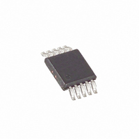
MAX1823AEUB+ Maxim Integrated Products, MAX1823AEUB+ Datasheet - Page 12

MAX1823AEUB+
Manufacturer Part Number
MAX1823AEUB+
Description
IC SW USB DUAL W/FB 10-UMAX
Manufacturer
Maxim Integrated Products
Datasheet
1.MAX1823BEUBT.pdf
(13 pages)
Specifications of MAX1823AEUB+
Applications
USB, Peripherals
Current - Supply
50µA
Voltage - Supply
4 V ~ 5.5 V
Operating Temperature
-40°C ~ 85°C
Mounting Type
Surface Mount
Package / Case
10-MSOP, Micro10™, 10-uMAX, 10-uSOP
Lead Free Status / RoHS Status
Lead free / RoHS Compliant
In the absence of faults, the MAX1823’s internal switches
turn on and off slowly under the control of the ON_
inputs. Transition times for both edges are provided in
the Electrical Characteristics table. The slow charge-
pump switch drive minimizes load transients on the
upstream power source. Under thermal fault and UVLO,
the power device turns off rapidly (100ns) to protect the
power device.
To optimize the switch response time to output short-
circuit conditions, keep all traces as short as possible
to reduce the effect of undesirable parasitic induc-
tance. Place input and output capacitors no more than
5mm from device leads. All IN_ and OUT_ pins must be
connected with short traces to the power bus. Wide
power-bus planes provide superior heat dissipation
through the switch IN_ and OUT_ pins.
While the switches are on, power dissipation is small, and
the package temperature change is minimal. Calculate
the power dissipation for this condition as follows:
For the normal operating current (I
the maximum on-resistance of the switch (135m ), the
power dissipation is:
The worst-case power dissipation occurs when the
switch is in current limit and the output is greater than
1V. In this case, the power dissipated in each switch is
the voltage drop across the switch multiplied by the
current limit:
Dual USB Switch with Fault
Blanking and Autoreset
12
______________________________________________________________________________________
P = (0.5A)
Layout and Thermal Dissipation
Turn-On and Turn-Off Behavior
P = (I
2
P = (I
x 0.135 = 34mW per switch
LIM
OUT_
) (V
IN
)
2
- V
R
ON
OUT
OUT_
)
= 0.5A), and
For a 5V input and 1V output, the maximum power dis-
sipation per switch is:
Since the package power dissipation is only 444mW,
the MAX1823 die temperature exceeds the thermal-
shutdown threshold, and the switch output shuts down
until the junction temperature cools by 15 C. The duty
cycle and period are strong functions of the ambient
temperature and the PC board layout.
A short circuit at the output causes the power dissipated
across the switch and the junction temperature to
increase. If the fault condition persists, the thermal-
overload-protection circuitry activates, and the output
shuts down until the junction temperature decreases by
15°C (see the Thermal Shutdown section).
Since the output short-circuit current is 25mA (typ), and
with V
short-circuited output as follows:
TRANSISTOR COUNT: 3227
PROCESS: BiCMOS
IN_
= 5V, calculate the power dissipation for a
P = (1.2A) ( 5V - 1V) = 4.8W
P = (0.025A)(5) = 0.125W
Chip Information


