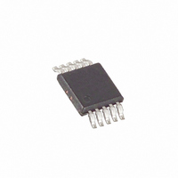
MAX1823AEUB+ Maxim Integrated Products, MAX1823AEUB+ Datasheet - Page 2

MAX1823AEUB+
Manufacturer Part Number
MAX1823AEUB+
Description
IC SW USB DUAL W/FB 10-UMAX
Manufacturer
Maxim Integrated Products
Datasheet
1.MAX1823BEUBT.pdf
(13 pages)
Specifications of MAX1823AEUB+
Applications
USB, Peripherals
Current - Supply
50µA
Voltage - Supply
4 V ~ 5.5 V
Operating Temperature
-40°C ~ 85°C
Mounting Type
Surface Mount
Package / Case
10-MSOP, Micro10™, 10-uMAX, 10-uSOP
Lead Free Status / RoHS Status
Lead free / RoHS Compliant
ABSOLUTE MAXIMUM RATINGS
IN, INA, INB, ONA, ONB, ONA, ONB
FAULTA, FAULTB to GND..........................-0.3V to (V
MAX1823/MAX1823H, INA, IN to OUTA;
MAX1823A/MAX1823B, INA, IN to OUTA;
INA, IN to OUTA; INB, IN to OUTB
Dual USB Switch with Fault
Blanking and Autoreset
ELECTRICAL CHARACTERISTICS
(Circuit of Figure 1, V
T
2
Stresses beyond those listed under “Absolute Maximum Ratings” may cause permanent damage to the device. These are stress ratings only, and functional
operation of the device at these or any other conditions beyond those indicated in the operational sections of the specifications is not implied. Exposure to
absolute maximum rating conditions for extended periods may affect device reliability.
A
Supply Voltage Range
Switch On-Resistance
Standby Supply Current
Quiescent Supply Current
OUT_ Off-Leakage Current
Undervoltage-Lockout Threshold
Continuous Load Current
Continuous Current Limit
Short-Circuit Current Limit
OUTA, OUTB to GND ...........................................-0.3V to +6V
INB, IN to OUTB ...................................................-0.3V to +6V
INB, IN to OUTB (when disabled, Note 3)...............-6V to +6V
(when enabled, Note 4)..............................-1.5A to +1.5A
= 0 C to +85 C, unless otherwise noted. Typical values are at T
_______________________________________________________________________________________
PARAMETER
IN
= V
INA
= V
INB
SYMBOL
I
V
SHORT
= 5V, ONA = ONB = GND (MAX1823/MAX1823A), ONA = ONB = IN (MAX1823B/MAX1823H),
R
UVLO
I
LIM
ON
T
MAX1823/MAX1823H
T
MAX1823A/MAX1823B
T
MAX1823/MAX1823H
T
MAX1823A/MAX1823B
ON_ = IN_ (MAX1823/MAX1823A), ON_ =
GND (MAX1823B/MAX1823H)
I
I
ON_ = IN _ ( MAX 1823/M AX1823A), ON _ = GND
(M AX1823B/M AX1823H), V
T
ON_ = IN_ (MAX1823/MAX1823A), ON_ =
GND (MAX1823B/MAX1823H),
V
Rising edge, 3% hysteresis
V
V
V
OUTA
OUTA
A
A
A
A
A
OUTA
IN
OUT_
OUT_
= +25°C, each switch,
= +25°C, each switch,
= 0°C to +85°C, each switch,
= 0°C to +85°C, each switch,
= +25
- V
IN_
= I
= I
OUT_
= 0V (I
= 0V (I
= V
+ 0.3V)
OUTB
OUTB
o
C
OUTB
RMS
= 0.5V
OUT
OUT
= 0A, one channel on
= 0A, both channels on
CONDITIONS
= 0V, T
A
pulsing)
pulsing)
= +25 C.)
FAULTA, FAULTB Current .................................................20mA
Continuous Power Dissipation (T
Operating Temperature Range ...........................-40 C to +85 C
Junction Temperature ......................................................+150 C
Storage Temperature Range .............................-65 C to +150 C
Lead Temperature (soldering, 10s) .................................+300 C
A
10-Pin µMAX (derate 5.6mW/ C above +70 C) ...........444mW
OUTA
= 0
o
C to +85
= V
OUTB
o
C
= 0V,
MIN
0.72
720
4.0
3.0
0.8
A
= +70 C)
TYP
0.02
0.02
0.90
0.35
3.4
1.2
75
90
40
50
3
10.00
MAX
1.00
1.20
105
120
135
165
100
5.5
3.8
1.6
10
80
UNITS
A
A
m
mA
PEAK
µA
µA
µA
RMS
V
V
A


