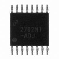
LM2702MT-ADJ/NOPB National Semiconductor, LM2702MT-ADJ/NOPB Datasheet

LM2702MT-ADJ/NOPB
Specifications of LM2702MT-ADJ/NOPB
*LM2702MT-ADJ/NOPB
LM2702MT-ADJ
Related parts for LM2702MT-ADJ/NOPB
LM2702MT-ADJ/NOPB Summary of contents
Page 1
... The LM2702 contains a Vcom amplifier and a Gamma buffer capable of supplying 50mA source and sink. The TSSOP-16 package ensures a low profile overall solution. Typical Application Circuit © 2005 National Semiconductor Corporation Features n 2A, 0.2Ω, internal power switch n V operating range: 2.2V to 12V ...
Page 2
Connection Diagram Pin Descriptions Pin Name 1 Vcom+ 2 Vcom− 3 Vcom 4 Delay 5 Css GND SWI 12 SWO 13 SWC GMA 16 ...
Page 3
... Ordering Information Order Number Package Type LM2702MT-ADJ LM2702MTX-ADJ lay capacitor, and compensation network to a dedicated AGND plane which connects directly to this pin. Connect all power ground components to a PGND plane which should also connect directly to this pin. Please see Layout Consid- erations under the Operation section for more details on layout suggestions ...
Page 4
Block Diagrams www.national.com 20051151 20051157 4 20051103 ...
Page 5
... Absolute Maximum Ratings If Military/Aerospace specified devices are required, please contact the National Semiconductor Sales Office/ Distributors for availability and specifications Voltage FB Voltage V Voltage C Css Voltage SWC Voltage Supply Voltage Amplifier/Buffer Input/Output Voltage Delay SWI Electrical Characteristics Switching Regulator Specifications in standard type face are for T ture Range ( T = − ...
Page 6
Electrical Characteristics Vcom Amplifier Specifications in standard type face are for T ture Range ( T = −40˚C to +125˚C). Unless otherwise specified 1nF. GAMMA Vcom Amplifier Symbol Parameter V Input Offset Voltage (Note OS 10) ...
Page 7
Electrical Characteristics Gamma Buffer Specifications in standard type face are for T ture Range ( T = −40˚C to +125˚C). Unless otherwise specified 1nF. GAMMA Gamma Buffer Symbol Parameter AV Supply Voltage IN Is+ Supply Current ...
Page 8
Typical Performance Characteristics Efficiency vs. Load Current (V = 8V) OUT Frequency vs. V Power Switch Current Limit vs. V www.national.com 20051126 Power Switch Current Limit vs. Temperature IN 20051125 IN 20051122 8 Efficiency vs. Load Current (V = 10V) ...
Page 9
Typical Performance Characteristics I vs (not switching) Feedback Current vs. Temperature Delay Current vs. V (Continued) 20051121 20051163 IN 20051165 (switching) 20051129 Soft Start Current vs 20051164 PMOS R ...
Page 10
Typical Performance Characteristics SWI Current vs. SWI Voltage (PMOS ON) Load Transient Response 2.5V OUT IN 1) Load, 20mA to 155mA to 20mA 200mV/div, AC OUT 500mA/div, DC ...
Page 11
Typical Performance Characteristics Internal Soft Start and PMOS Delay 2.5V 40Ω none OUT IN LOAD 100nF 10k\1.5k, SWI = 30V, SWC = ...
Page 12
Typical Performance Characteristics Input Bias Current vs. Common Mode Voltage (Vcom) Output Voltage vs. Output Current (Vcom or Gamma, sinking) Supply Current vs. Common Mode Voltage (Both Amplifiers) www.national.com (Continued) Input Bias Current vs. Common Mode Voltage 20051178 Output Voltage ...
Page 13
Typical Performance Characteristics Large Signal Step Response (no ext. compensation) Negative Slew Rate vs. Capacitive Load (Vcom or Gamma) Unity Gain Frequency vs. Capacitive Load (Vcom) (Continued) Positive Slew Rate vs. Capacitive Load 20051184 Phase Margin vs. Capacitive Load 20051185 ...
Page 14
Typical Performance Characteristics www.national.com (Continued) PSRR vs. Frequency (Vcom) 20051189 14 ...
Page 15
Operation FIGURE 1. Simplified Boost Converter Diagram (a) First Cycle of Operation (b) Second Cycle Of Operation CONTINUOUS CONDUCTION MODE The LM2702 is a TFT Panel Module containing a current- mode, PWM boost regulator. A boost regulator steps the input ...
Page 16
Operation (Continued) section, the soft start curent has a temperature coefficient and would lead one to believe there would be significant variation with temperature. Though the current has a tem- perature coefficient the actual programmed external soft start time does ...
Page 17
Operation (Continued) where R is the output impedance of the error amplifier, O approximately 1MΩ. For most applications, performance can be optimized by choosing values within the range 5kΩ ≤ R ≤ 40kΩ (R can 200kΩ if ...
Page 18
Operation (Continued) Where R is the minimum load resistance corresponding to L the maximum load current. The zero created by the ESR of the output capacitor is generally very high frequency if the ESR is small. If low ESR capacitors ...
Page 19
Operation (Continued) Vcom AND Gamma COMPENSATION The architecture used for the amplifiers in the LM2702 re- quires external compensation on the output. Depending on the equivalent capacitive load of the TFT-LCD panel, exter- nal components at the amplifier outputs may ...
Page 20
Operation (Continued) Application Information www.national.com FIGURE 4. Single Layer Layout FIGURE 10V TFT Application 20 20051153 20051172 ...
Page 21
... BANNED SUBSTANCE COMPLIANCE National Semiconductor manufactures products and uses packing materials that meet the provisions of the Customer Products Stewardship Specification (CSP-9-111C2) and the Banned Substances and Materials of Interest Specification (CSP-9-111S2) and contain no ‘‘Banned Substances’’ as defined in CSP-9-111S2. ...


