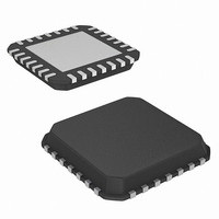
ISL6532ACR Intersil, ISL6532ACR Datasheet - Page 14

ISL6532ACR
Manufacturer Part Number
ISL6532ACR
Description
IC REG/CTRLR ACPI DUAL DDR 28QFN
Manufacturer
Intersil
Datasheet
1.ISL6532ACRZ.pdf
(17 pages)
Specifications of ISL6532ACR
Applications
Memory, DDR/DDR2 Regulator
Current - Supply
5.25mA
Operating Temperature
0°C ~ 70°C
Mounting Type
Surface Mount
Package / Case
28-QFN
Lead Free Status / RoHS Status
Contains lead / RoHS non-compliant
Voltage - Supply
-
Available stocks
Company
Part Number
Manufacturer
Quantity
Price
Part Number:
ISL6532ACR
Manufacturer:
INTERS
Quantity:
20 000
Company:
Part Number:
ISL6532ACR-T
Manufacturer:
TOSHIBA
Quantity:
1 355
Part Number:
ISL6532ACR-T
Manufacturer:
INTERSIL
Quantity:
20 000
Part Number:
ISL6532ACRZ
Manufacturer:
INTERSIZ
Quantity:
20 000
Company:
Part Number:
ISL6532ACRZ-T
Manufacturer:
INTERSIL
Quantity:
6 000
To properly compensate the LDO system, a 100kΩ 1%
resistor and a 680pF X5R ceramic capacitor, represented as
R
insure a stable system with any MOSFET given the following
conditions:
Maximum bandwidth will be realized at full load while
minimum bandwidth will be realized at no load. Bandwidth at
no load will be maximized as τ becomes closer to 10μs.
Output Voltage Selection
The output voltage of the V
programmed to any level between V
reference, 0.8V. An external resistor divider is used to scale
the output voltage relative to the reference voltage and feed
it back to the inverting input of the error amplifier, see
Figure 5. However, since the value of R
the rest of the compensation components, it is advisable to
keep its value less than 5kΩ. Depending on the value chosen
for R
If the output voltage desired is 0.8V, simply route V
to the FB pin through R
The output voltage for the internal V
internal to the ISL6532A to track the V
There is no need for external programming resistors.
As with the V
output voltage is set by means of an external resistor divider
as shown in Figure 7. For stability concerns described
earlier, the recommended value of the feedback resistor, R
is 249Ω. The voltage programming resistor, R
calculated based on the Equation 8:
R
τ
R
R
10
4
FB
9
FIGURE 7. COMPENSATION AND OUTPUT VOLTAGE
=
REFERENCE
=
and C
=
C
1
=
, R
OUT
----------------------------------- -
V
0.8V
---------------------------------- -
V
R
R
R1
DDQ
R
AGP
4
9
8
8
25
can be calculated based on the Equation 7:
⋅
×
×
=
+
-
ESR
0.8V
0.8V
- 0.8V
- 0.8V
DDQ
in Figure 7, are used. This compensation will
249Ω
ISL6532A
SELECTION OF THE LINEAR
V
IMPEDANCE
AGP
>
FB2
OUTPUT
PWM regulator, the AGP linear regulator
10μs
650Ω
=
0.8
1
, but do not populate R
×
DDQ
DRIVE2
⎛
⎜
⎝
C
14
1
25
+
PWM converter can be
R
------ -
R
8
9
⎞
⎟
⎠
TT
IN
DDQ
R
1
and the internal
linear regulator is set
10
affects the values of
R
C
8
voltage by 50%.
ESR
OUT
9
V
can be
4
DDQ
.
+
DDQ
V
(EQ. 7)
(EQ. 8)
(EQ. 6)
R
AGP
back
LOAD
ISL6532A
8
,
Component Selection Guidelines
Output Capacitor Selection - PWM Buck Converter
An output capacitor is required to filter the inductor current
and supply the load transient current. The filtering
requirements are a function of the switching frequency and
the ripple current. The load transient requirements are a
function of the slew rate (di/dt) and the magnitude of the
transient load current. These requirements are generally met
with a mix of capacitors and careful layout.
DDR memory systems are capable of producing transient
load rates above 1A/ns. High frequency capacitors initially
supply the transient and slow the current load rate seen by
the bulk capacitors. The bulk filter capacitor values are
generally determined by the ESR (Effective Series
Resistance) and voltage rating requirements rather than
actual capacitance requirements.
High frequency decoupling capacitors should be placed as
close to the power pins of the load as physically possible. Be
careful not to add inductance in the circuit board wiring that
could cancel the usefulness of these low inductance
components. Consult with the manufacturer of the load on
specific decoupling requirements.
Use only specialized low-ESR capacitors intended for
switching-regulator applications for the bulk capacitors. The
bulk capacitor’s ESR will determine the output ripple voltage
and the initial voltage drop after a high slew-rate transient.
An aluminum electrolytic capacitor’s ESR value is related to
the case size with lower ESR available in larger case sizes.
However, the Equivalent Series Inductance (ESL) of these
capacitors increases with case size and can reduce the
usefulness of the capacitor to high slew-rate transient
loading. Unfortunately, ESL is not a specified parameter.
Work with your capacitor supplier and measure the
capacitor’s impedance with frequency to select a suitable
component. In most cases, multiple electrolytic capacitors of
small case size perform better than a single large case
capacitor.
Output Capacitor Selection - LDO Regulators
The output capacitors used in LDO regulators are used to
provide dynamic load current. The amount of capacitance
and type of capacitor should be chosen with this criteria in
mind.
Output Inductor Selection
The output inductor is selected to meet the output voltage
ripple requirements and minimize the converter’s response
time to the load transient. The inductor value determines the
converter’s ripple current and the ripple voltage is a function
of the ripple current. The ripple voltage and current are
approximated by the following equations:
ΔI =
V
IN
Fs x L
- V
OUT
x
V
V
OUT
IN
ΔV
OUT
= ΔI x ESR
May 5, 2008
(EQ. 9)
FN9099.5


