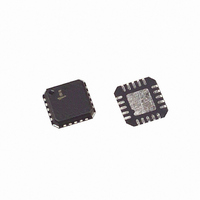
ISL6532BCR Intersil, ISL6532BCR Datasheet - Page 13

ISL6532BCR
Manufacturer Part Number
ISL6532BCR
Description
IC REG/CTRLR ACPI DUAL DDR 20QFN
Manufacturer
Intersil
Datasheet
1.ISL6532BCRZ.pdf
(15 pages)
Specifications of ISL6532BCR
Applications
Memory, DDR/DDR2 Regulator
Current - Supply
5.25mA
Operating Temperature
0°C ~ 70°C
Mounting Type
Surface Mount
Package / Case
20-QFN
Lead Free Status / RoHS Status
Contains lead / RoHS non-compliant
Voltage - Supply
-
I
The important parameters for the bulk input capacitance are
the voltage rating and the RMS current rating. For reliable
operation, select bulk capacitors with voltage and current
ratings above the maximum input voltage and largest RMS
current required by the circuit. Their voltage rating should be
at least 1.25 times greater than the maximum input voltage,
while a voltage rating of 1.5 times is a conservative
guideline. For worst cases, the RMS current rating
requirement for the input capacitor of a buck regulator is
approximately 1/2 the DC output load current.
The maximum RMS current required by the regulator may be
closely approximated through the following equation:
For a through hole design, several electrolytic capacitors
may be needed. For surface mount designs, solid tantalum
capacitors can be used, but caution must be exercised with
regard to the capacitor surge current rating. These
capacitors must be capable of handling the surge-current at
power-up. Some capacitor series available from reputable
manufacturers are surge current tested.
MOSFET Selection - PWM Buck Converter
The ISL6532B requires 2 N-Channel power MOSFETs for
switching power and a third MOSFET to block backfeed from
V
based upon r
management requirements.
RMS
DDQ
MAX
to the Input in S3 Mode. These should be selected
=
DS(ON)
V
--------------- -
V
OUT
IN
×
, gate supply requirements, and thermal
I
OUT
MAX
13
2
+
----- -
12
1
×
V
------------------------------- -
IN
L f
–
×
V
sw
OUT
×
V
--------------- -
V
OUT
IN
ISL6532B
2
In high-current applications, the MOSFET power dissipation,
package selection and heatsink are the dominant design
factors. The power dissipation includes two loss
components; conduction loss and switching loss. The
conduction losses are the largest component of power
dissipation for both the upper and the lower MOSFETs.
These losses are distributed between the two MOSFETs
according to duty factor. The switching losses seen when
sourcing current will be different from the switching losses
seen when sinking current. When sourcing current, the
upper MOSFET realizes most of the switching losses. The
lower switch realizes most of the switching losses when the
converter is sinking current (see the equations below).
These equations assume linear voltage-current transitions
and do not adequately model power loss due the reverse-
recovery of the upper and lower MOSFET’s body diode. The
gate-charge losses are dissipated in part by the ISL6532B
and do not significantly heat the MOSFETs. However, large
gate-charge increases the switching interval, tSW which
increases the MOSFET switching losses. Ensure that both
MOSFETs are within their maximum junction temperature at
high ambient temperature by calculating the temperature
rise according to package thermal-resistance specifications.
A separate heatsink may be necessary depending upon
MOSFET power, package type, ambient temperature and air
flow.
Approximate Losses while Sinking current
Approximate Losses while Sourcing current
P
P
P
P
LOWER
UPPER
UPPER
LOWER
Where: D is the duty cycle = V
= Io
= Io
=
=
t
f
SW
s
Io
2
Io
is the switching frequency.
2
2
x r
x r
2
is the combined switch ON and OFF time, and
×
×
DS(ON)
DS(ON)
r
r
DS ON
DS ON
(
(
x D
x (1 - D)
)
)
×
×
D
(
1 D
+
–
1
-- - Io
2
OUT
⋅
)
+
/ V
×
1
-- - Io
2
V
⋅
IN
IN
,
×
×
V
t
SW
IN
×
×
t
f
SW
s
×
f
s


