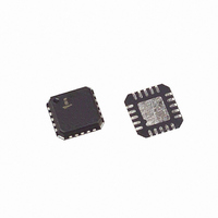
ISL6532BCR-T Intersil, ISL6532BCR-T Datasheet - Page 11

ISL6532BCR-T
Manufacturer Part Number
ISL6532BCR-T
Description
IC REG/CTRLR ACPI DUAL DDR 20QFN
Manufacturer
Intersil
Datasheet
1.ISL6532BCRZ.pdf
(15 pages)
Specifications of ISL6532BCR-T
Applications
Memory, DDR/DDR2 Regulator
Current - Supply
5.25mA
Operating Temperature
0°C ~ 70°C
Mounting Type
Surface Mount
Package / Case
20-QFN
Lead Free Status / RoHS Status
Contains lead / RoHS non-compliant
Voltage - Supply
-
The compensation network consists of the error amplifier
(internal to the ISL6532B) and the impedance networks Z
and Z
a closed loop transfer function with the highest 0dB crossing
frequency (f
is the difference between the closed loop phase at f
180 degrees. The equations below relate the compensation
network’s poles, zeros and gain to the components (R
R
locating the poles and zeros of the compensation network:
V
∆V
1. Pick Gain (R
3. Place 2
4. Place 1
5. Place 2
6. Check Gain against Error Amplifier’s Open-Loop Gain.
7. Estimate Phase Margin - Repeat if Necessary.
2. Place 1
3
DDQ
FIGURE 5. VOLTAGE-MODE BUCK CONVERTER
OSC
, C
FB
1
=
, C
. The goal of the compensation network is to provide
OSC
0.8
2
ST
, and C
ND
ST
ND
0dB
×
COMPARATOR
COMPENSATION DESIGN AND OUTPUT
VOLTAGE SELECTION
Zero Below Filter’s Double Pole (~75% F
ERROR
AMP
DETAILED COMPENSATION COMPONENTS
Pole at the ESR Zero.
V
1
Zero at Filter’s Double Pole.
Pole at Half the Switching Frequency.
ISL6532B
) and adequate phase margin. Phase margin
E/A
+
2
PWM
/R
R
------ -
R
3
Z
+
-
) in Figure 5. Use these guidelines for
1
4
1
FB
-
+
COMP
) for desired converter bandwidth.
C
REFERENCE
2
REFERENCE
C
-
+
1
DRIVER
DRIVER
R
11
Z
2
IN
FB
Z
FB
PHASE
R
(PARASITIC)
V
4
C
IN
3
L
Z
R
IN
O
1
R
ESR
C
3
O
V
DDQ
0dB
LC
V
1
DDQ
, R
).
and
IN
2
ISL6532B
,
Compensation Break Frequency Equations
Figure 6 shows an asymptotic plot of the DC-DC converter’s
gain vs frequency. The actual Modulator Gain has a high
gain peak due to the high Q factor of the output filter and is
not shown in Figure 6. Using the above guidelines should
give a Compensation Gain similar to the curve plotted. The
open loop error amplifier gain bounds the compensation
gain. Check the compensation gain at FP2 with the
capabilities of the error amplifier. The Closed Loop Gain is
constructed on the graph of Figure 6 by adding the
Modulator Gain (in dB) to the Compensation Gain (in dB).
This is equivalent to multiplying the modulator transfer
function to the compensation transfer function and plotting
the gain.
The compensation gain uses external impedance networks
Z
loop. A stable control loop has a gain crossing with
-20dB/decade slope and a phase margin greater than 45
degrees. Include worst case component variations when
determining phase margin.
Output Voltage Selection
The output voltage of the VDDQ PWM converter can be
programmed to any level between VIN and the internal
reference, 0.8V. An external resistor divider is used to scale
the output voltage relative to the reference voltage and feed
it back to the inverting input of the error amplifier, see
Figure 6.
FIGURE 6. ASYMPTOTIC BODE PLOT OF CONVERTER GAIN
FB
100
-20
-40
-60
F
F
80
60
40
20
Z1
Z2
0
and Z
=
=
10
(R
20LOG
----------------------------------- -
2π x R
------------------------------------------------------ -
2π x R
MODULATOR
2
IN
/R
1
to provide a stable, high bandwidth (BW) overall
GAIN
)
100
(
1
2
1
x C
+
1
R
2
3
1K
F
) x C
Z1
F
FREQUENCY (Hz)
LC
F
Z2
3
10K
F
F
F
F
P1
ESR
P1
P2
(V
100K
IN
20LOG
F
=
=
/∆V
P2
-------------------------------------------------------- -
2π x R
----------------------------------- -
2π x R
OSC
OPEN LOOP
ERROR AMP GAIN
)
1M
1
2
3
COMPENSATION
x
x C
CLOSED LOOP
1
10M
C
--------------------- -
C
GAIN
3
GAIN
1
1
x C
+
C
2
2


