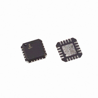
ISL6532BCR-T Intersil, ISL6532BCR-T Datasheet - Page 12

ISL6532BCR-T
Manufacturer Part Number
ISL6532BCR-T
Description
IC REG/CTRLR ACPI DUAL DDR 20QFN
Manufacturer
Intersil
Datasheet
1.ISL6532BCRZ.pdf
(15 pages)
Specifications of ISL6532BCR-T
Applications
Memory, DDR/DDR2 Regulator
Current - Supply
5.25mA
Operating Temperature
0°C ~ 70°C
Mounting Type
Surface Mount
Package / Case
20-QFN
Lead Free Status / RoHS Status
Contains lead / RoHS non-compliant
Voltage - Supply
-
However, since the value of R1 affects the values of the rest of
the compensation components, it is advisable to keep its
value less than 5kΩ. Depending on the value chosen for R1,
R4 can be calculated based on the following equation:
If the output voltage desired is 0.8V, simply route V
to the FB pin through R1, but do not populate R4.
The output voltage for the internal V
internal to the ISL6532B to track the V
There is no need for external programming resistors.
Component Selection Guidelines
Output Capacitor Selection - PWM Buck Converter
An output capacitor is required to filter the inductor current
and supply the load transient current. The filtering
requirements are a function of the switching frequency and
the ripple current. The load transient requirements are a
function of the slew rate (di/dt) and the magnitude of the
transient load current. These requirements are generally met
with a mix of capacitors and careful layout.
DDR memory systems are capable of producing transient
load rates above 1A/ns. High frequency capacitors initially
supply the transient and slow the current load rate seen by the
bulk capacitors. The bulk filter capacitor values are generally
determined by the ESR (Effective Series Resistance) and
voltage rating requirements rather than actual capacitance
requirements.
High frequency decoupling capacitors should be placed as
close to the power pins of the load as physically possible. Be
careful not to add inductance in the circuit board wiring that
could cancel the usefulness of these low inductance
components. Consult with the manufacturer of the load on
specific decoupling requirements.
Use only specialized low-ESR capacitors intended for
switching-regulator applications for the bulk capacitors. The
bulk capacitor’s ESR will determine the output ripple voltage
and the initial voltage drop after a high slew-rate transient. An
aluminum electrolytic capacitor’s ESR value is related to the
case size with lower ESR available in larger case sizes.
However, the Equivalent Series Inductance (ESL) of these
capacitors increases with case size and can reduce the
usefulness of the capacitor to high slew-rate transient loading.
Unfortunately, ESL is not a specified parameter. Work with
your capacitor supplier and measure the capacitor’s
impedance with frequency to select a suitable component. In
most cases, multiple electrolytic capacitors of small case size
perform better than a single large case capacitor.
R4
=
---------------------------------- -
V
R1
DDQ
×
–
0.8V
0.8V
12
TT
DDQ
linear regulator is set
voltage by 50%.
DDQ
back
ISL6532B
Output Capacitor Selection - LDO Regulator
The output capacitors used in LDO regulators are used to
provide dynamic load current. The amount of capacitance
and type of capacitor should be chosen with this criteria in
mind.
Output Inductor Selection
The output inductor is selected to meet the output voltage
ripple requirements and minimize the converter’s response
time to the load transient. The inductor value determines the
converter’s ripple current and the ripple voltage is a function
of the ripple current. The ripple voltage and current are
approximated by the following equations:
Increasing the value of inductance reduces the ripple current
and voltage. However, the large inductance values reduce
the converter’s response time to a load transient.
One of the parameters limiting the converter’s response to a
load transient is the time required to change the inductor
current. Given a sufficiently fast control loop design, the
ISL6532B will provide either 0% or 100% duty cycle in
response to a load transient. The response time is the time
required to slew the inductor current from an initial current
value to the transient current level. During this interval the
difference between the inductor current and the transient
current level must be supplied by the output capacitor.
Minimizing the response time can minimize the output
capacitance required.
The response time to a transient is different for the
application of load and the removal of load. The following
equations give the approximate response time interval for
application and removal of a transient load:
where: I
response time to the application of load, and t
response time to the removal of load. The worst case
response time can be either at the application or removal of
load. Be sure to check both of these equations at the
minimum and maximum output levels for the worst case
response time.
Input Capacitor Selection - PWM Buck Converter
Use a mix of input bypass capacitors to control the voltage
overshoot across the MOSFETs. Use small ceramic
capacitors for high frequency decoupling and bulk capacitors
to supply the current needed each time the upper MOSFET
turns on. Place the small ceramic capacitors physically close
to the MOSFETs, between the drain of upper MOSFET and
the source of lower MOSFET.
∆I =
t
RISE
=
V
IN
TRAN
Fs x L
V
- V
L x I
IN
OUT
- V
is the transient load current step, t
TRAN
OUT
x
V
V
OUT
IN
t
FALL
∆V
OUT
=
L x I
= ∆I x ESR
V
OUT
TRAN
FALL
RISE
is the
is the


