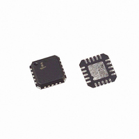
ISL6532BCR-T Intersil, ISL6532BCR-T Datasheet - Page 6

ISL6532BCR-T
Manufacturer Part Number
ISL6532BCR-T
Description
IC REG/CTRLR ACPI DUAL DDR 20QFN
Manufacturer
Intersil
Datasheet
1.ISL6532BCRZ.pdf
(15 pages)
Specifications of ISL6532BCR-T
Applications
Memory, DDR/DDR2 Regulator
Current - Supply
5.25mA
Operating Temperature
0°C ~ 70°C
Mounting Type
Surface Mount
Package / Case
20-QFN
Lead Free Status / RoHS Status
Contains lead / RoHS non-compliant
Voltage - Supply
-
Electrical Specifications
Functional Pin Description
5VSBY (Pin 1)
5VSBY is the bias supply of the ISL6532B. It is typically
connected to the 5V standby rail of an ATX power supply.
During S4/S5 sleep states the ISL6532B enters a reduced
power mode and draws less than 1mA (I
5VSBY supply. This pin should be locally bypassed using a
0.1µF capacitor.
P12V (Pin 18)
P12V provides the gate drive current to the switching
MOSFETs of the PWM power stage. The V
circuit is also powered by P12V. P12V is only required during
S0/S1/S2 operation. P12V is typically connected to the +12V
rail of an ATX power supply.
PWM CONTROLLER GATE DRIVERS
UGATE and LGATE Source
UGATE and LGATE Sink
NCH BACKFEED CONTROL
NCH Current Sink
NCH Trip Level
VDDQ STANDBY LDO
Output Drive Current
VTT REGULATOR
Upper Divider Impedance
Lower Divider Impedance
VREF_OUT Buffer Source Current
Maximum V
VTT Over Current Trip
PGOOD
PGOOD Rising Threshold
PGOOD Falling Threshold
PROTECTION
VDDQ OV Level
VDDQ UV Level
Thermal Shutdown Limit
TT
PARAMETER
Load Current
6
Recommended Operating Conditions, Unless Otherwise Noted. Refer to Block and Simplified Power System
Diagrams and Typical Application Schematics (Continued)
CC5
V
V
VTTSNS/
VTTSNS/
TT
I
) from the
VREF_OUT
I
V
V
I
SYMBOL
VTT_MAX
TRIP_VTT
FB
FB
regulation
I
I
V
I
GATE
GATE
T
NCH
R
NCH
R
/V
/V
SD
U
L
REF
REF
V
V
VDDQ
VDDQ
ISL6532B
NCH = 0.8V
P5VSBY = 5.0V
P5VSBY = 3.3V
Periodic load applied with 30% duty cycle
and 10ms period using ISL6532EVAL1
evaluation board (see Application Note
AN1055)
By Design
S3# & S5# HIGH
S3# & S5# HIGH
S3# & S5# HIGH
S3# & S5# HIGH
By Design
TEST CONDITIONS
P5VSBY (Pin 8)
This pin provides the V
sleep state. The regulator is capable of providing standby
V
GND (Pin 2, 13, 21)
The GND terminals of the ISL6532B provide the return path
for the V
drivers. High ground currents are conducted directly through
the exposed paddle of the QFN package which must be
electrically connected to the ground plane through a path as
low in inductance as possible.
UGATE (Pin 20)
UGATE drives the upper (control) FET of the V
synchronous buck switching regulator. UGATE is driven
between GND and P12V.
DDQ
power from either a 5V or 3.3V source.
TT
LDO, Standby LDO and switching MOSFET gate
DDQ
output power during the S3
MIN
-3.3
9.0
-3
-
-
-
-
-
-
-
-
-
-
-
-
-
TYP
57.5
45.0
-0.8
115
140
0.8
9.5
2.5
2.5
85
-
-
-
-
-
-
MAX
650
550
3.3
10
6
2
3
-
-
-
-
-
-
-
-
-
DDQ
UNITS
mA
mA
mA
mA
kΩ
kΩ
°C
%
%
%
%
A
A
V
A
A


