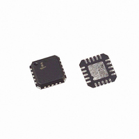
ISL6532BCR-T Intersil, ISL6532BCR-T Datasheet - Page 9

ISL6532BCR-T
Manufacturer Part Number
ISL6532BCR-T
Description
IC REG/CTRLR ACPI DUAL DDR 20QFN
Manufacturer
Intersil
Datasheet
1.ISL6532BCRZ.pdf
(15 pages)
Specifications of ISL6532BCR-T
Applications
Memory, DDR/DDR2 Regulator
Current - Supply
5.25mA
Operating Temperature
0°C ~ 70°C
Mounting Type
Surface Mount
Package / Case
20-QFN
Lead Free Status / RoHS Status
Contains lead / RoHS non-compliant
Voltage - Supply
-
V
The internal V
through a 3.3A current limit. This current limit protects the
ISL6532B if the LDO is sinking or sourcing current. During
an overcurrent event on the V
disabled. Once the over current condition on the V
removed, V
Over/Under Voltage Protection
Both the internal V
protected from faults through internal Over/Under voltage
detection circuitry. If either rail falls below 85% of the targeted
voltage, then an undervoltage event is tripped. An under
voltage will disable all regulators for a period of 3 soft-start
cycles, after which a normal soft-start is initiated. If the output
remains under 85% of target, the regulators will continue to be
disabled and soft-started in a hiccup mode until the fault is
cleared. See Figure 3.
If either rail exceeds 115% of the targeted voltage, then all
outputs are immediately disabled. The ISL6532B will not re-
enable the outputs until either the bias voltage is toggled in
order to initiate a POR or the SLP_S5 signal is forced LOW
and then back to HIGH.
Thermal Protection (S0/S3 State)
If the ISL6532B IC junction temperature reaches a nominal
temperature of 140
ISL6532B will not re-enable the outputs until the junction
temperature drops below 110
is toggled in order to initiate a POR or the SLP_S5 signal is
forced LOW and then back to HIGH.
S3
S5
TT
Over Current Protection
FIGURE 2. TYPICAL S3 TO S0 STATE TRANSITION
TT
TT
will recover.
12V POR
LDO is protected from fault conditions
TT
o
C, all regulators will be disabled. The
LDO and the V
2048 CLOCK
CYCLES
12VATX 2V/DIV
o
TT
9
C and either the bias voltage
PGOOD COMPARATOR
LDO, only the V
DDQ
.
ENABLED
regulator are
500mV/DIV
500mV/DIV
PGOOD
TT
5V/DIV
V
V
TT
DDQ
TT
LDO is
rail is
ISL6532B
Shoot-Through Protection
A shoot-through condition occurs when both the upper and
lower MOSFETs are turned on simultaneously, effectively
shorting the input voltage to ground. To protect from a shoot-
through condition, the ISL6532B incorporates specialized
circuitry which insures that complementary MOSFETs are
not ON simultaneously.
The adaptive shoot-through protection utilized by the V
regulator looks at the lower gate drive pin, LGATE, and the
upper gate drive pin, UGATE, to determine whether a
MOSFET is ON or OFF. If the voltage from UGATE or from
LGATE to GND is less than 0.8V, then the respective
MOSFET is defined as being OFF and the other MOSFET is
allowed to be turned ON. This method allows the V
regulator to both source and sink current.
Since the voltage of the MOSFET gates are being measured
to determine the state of the MOSFET, the designer is
encouraged to consider the repercussions of introducing
external components between the gate drivers and their
respective MOSFET gates before actually implementing
such measures. Doing so may interfere with the shoot-
through protection.
Application Guidelines
Layout Considerations
Layout is very important in high frequency switching
converter design. With power devices switching efficiently at
250kHz, the resulting current transitions from one device to
another cause voltage spikes across the interconnecting
impedances and parasitic circuit elements. These voltage
FIGURE 3. V
V
V
DDQ
TT
T0
RESPONSES
TT
/V
DELAY INTERVAL
INTERNAL DELAY
DDQ
LDO UNDER VOLTAGE PROTECTION
500mV/DIV
TIME
T1
DDQ
T2
DDQ


