ISL6532CCR-T Intersil, ISL6532CCR-T Datasheet
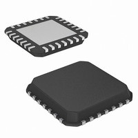
IC REG/CTRLR ACPI DUAL DDR 28QFN

ISL6532CCR-T

Manufacturer Part Number
ISL6532CCR-T
Description
IC REG/CTRLR ACPI DUAL DDR 28QFN
Manufacturer
Intersil
Datasheet

Specifications of ISL6532CCR-T

Applications
Memory, DDR/DDR2 Regulator
Current - Supply
5.25mA
Operating Temperature
0°C ~ 70°C
Mounting Type
Surface Mount
Package / Case
28-QFN
Lead Free Status / RoHS Status
Contains lead / RoHS non-compliant
Voltage - Supply
-
ACPI Regulator/Controller for
Dual Channel DDR Memory Systems
The ISL6532C provides a complete ACPI compliant power
solution for up to 4 DIMM dual channel DDR/DDR2 Memory
systems. Included are both a synchronous buck controller
and integrated LDO to supply V
S0/S1 states and standby current during S3 state. During
S0/S1 state, a fully integrated sink-source regulator
generates an accurate (V
without the need for a negative supply. A buffered version of
the V
controller is also integrated for AGP core voltage regulation.
The switching PWM controller drives two N-Channel
MOSFETs in a synchronous-rectified buck converter
topology. The synchronous buck converter uses voltage-
mode control with fast transient response. Both the switching
regulator and standby LDO provide a maximum static
regulation tolerance of
ranges. The output is user-adjustable by means of external
resistors down to 0.8V.
Switching memory core output between the PWM regulator
and the standby LDO during state transitions is
accomplished smoothly via the internal ACPI control
circuitry. The NCH signal provides synchronized switching of
a backfeed blocking switch during the transitions eliminating
the need to route 5V Dual to the memory supply.
An integrated soft-start feature brings all outputs into
regulation in a controlled manner when returning to S0/S1
state from any sleep state. During S0 the PGOOD signal
indicates V
Each output is monitored for under and over-voltage events.
The switching regulator has over current protection. Thermal
shutdown is integrated.
Pinout
DDQ
5VSBY
GNDQ
GNDQ
GNDP
VDDQ
/2 reference is provided as V
VTT
VTT
TT
is within spec and operational.
1
2
3
4
5
6
7
ISL6532C (QFN) TOP VIEW
28 27 26 25 24 23 22
8
9
±
2% over line, load, and temperature
DDQ
10 11 12 13 14
®
/2) high current V
1
DDQ
Data Sheet
with high current during
REF
. An LDO
21
20
19
18
17
16
15
PGOOD
PHASE
DRIVE2
FB2
GNDA
COMP
FB
TT
voltage
1-888-INTERSIL or 321-724-7143
CAUTION: These devices are sensitive to electrostatic discharge; follow proper IC Handling Procedures.
Features
• Generates 3 Regulated Voltages
• ACPI compliant sleep state control
• Integrated V
• PWM Controller Drives Low Cost N-Channel MOSFETs
• 250kHz Constant Frequency Operation
• Tight Output Voltage Regulation
• 5V or 3.3V Down Conversion
• Fully-Adjustable Outputs with Wide Voltage Range: Down
• Simple Single-Loop Voltage-Mode PWM Control Design
• Fast PWM Converter Transient Response
• Under and Over-voltage Monitoring on All Outputs
• OCP on the Switching Regulator and V
• Integrated Thermal Shutdown Protection
• QFN Package Option
• Pb-free available
Applications
• Single and Dual Channel DDR Memory Power Systems in
• Graphics cards - GPU and memory supplies
• ASIC power supplies
• Embedded processor and I/O supplies
• DSP supplies
Ordering Information
ISL6532CCR
ISL6532CCRZ
(See Note)
*Add “-T” suffix to part number for tape and reel packaging.
NOTE: Intersil Pb-free products employ special Pb-free material sets; molding
compounds/die attach materials and 100% matte tin plate termination finish, which
is compatible with both SnPb and Pb-free soldering operations. Intersil Pb-free
products are MSL classified at Pb-free peak reflow temperatures that meet or
exceed the Pb-free requirements of IPC/JEDEC J Std-020B.
PART NUMBER
- Synchronous Buck PWM Controller with Standby LDO
- 3A Integrated Sink/Source Linear Regulator with
- Glitch-free Transitions During State Changes
- LDO Regulator for 1.5V Video and Core voltage
- All Outputs:
to 0.8V supports DDR and DDR2 Specifications
- QFN Compliant to JEDEC PUB95 MO-220 QFN - Quad
- QFN Near Chip Scale Package Footprint; Improves
ACPI compliant PCs
Accurate VDDQ/2 Divider Reference.
Flat No Leads - Product Outline
PCB Efficiency, Thinner in Profile
All other trademarks mentioned are the property of their respective owners.
|
Intersil (and design) is a registered trademark of Intersil Americas Inc.
Copyright © Intersil Americas Inc. 2002-2004. All Rights Reserved.
July 2004
REF
±
TEMP. RANGE
2% Over Temperature
Buffer
0 to 70
0 to 70
(
o
C)
28 Ld 6x6 QFN L28.6x6
28 Ld 6x6 QFN
(Pb-free)
PACKAGE
ISL6532C
TT
FN9121.2
L28.6x6
PKG. DWG. #

Related parts for ISL6532CCR-T

ISL6532CCR-T Summary of contents

Page 1

... PART NUMBER 17 GNDA ISL6532CCR 16 COMP ISL6532CCRZ (See Note *Add “-T” suffix to part number for tape and reel packaging. NOTE: Intersil Pb-free products employ special Pb-free material sets; molding compounds/die attach materials and 100% matte tin plate termination finish, which is compatible with both SnPb and Pb-free soldering operations. Intersil Pb-free products are MSL classified at Pb-free peak reflow temperatures that meet or exceed the Pb-free requirements of IPC/JEDEC J Std-020B ...

Page 2

Block Diagram P5VSBY VDDQ S3 REGULATOR + - VDDQ(3) VTTSNS VTT REG - VTT(2) + GNDQ DISABLE { R U VREF_IN { GNDA + - UV/OV2 VREF_OUT S3# S5# 5VSBY VOLTAGE REFERENCE 0.800V 0.680V (-15%) 5V ...

Page 3

Simplified Power System Diagram SLP_S3 SLP_S5 5VSBY/3V3SBY V DDQ Q3 V AGP + Typical Application - 5V or 3.3V Input +3.3V PGOOD V DDQ SLP_S3 SLP_S5 V REF VTT_OUT V DDQ Q3 V AGP 1.5V + ...

Page 4

Typical Application - Input From 5V Dual +3.3V PGOOD V DDQ SLP_S3 SLP_S5 V REF VTT_OUT V DDQ Q3 V AGP 1. OUT2 4 ISL6532C 5VSBY +12V C BP S3# NCH S5# VREF_OUT OCSET ...

Page 5

Absolute Maximum Ratings 5VSBY, P5VSBY . . . . . . . . . . . . . . . . . . . . . . . . . GND - 0.3V to +7V P12V . . . . ...

Page 6

Electrical Specifications Recommended Operating Conditions, Unless Otherwise Noted. Refer to Block and Simplified Power System Diagrams and Typical Application Schematics (Continued) PARAMETER PWM CONTROLLER GATE DRIVERS UGATE and LGATE Source UGATE and LGATE Sink NCH BACKFEED CONTROL NCH Current Sink ...

Page 7

Functional Pin Description 5VSBY (Pin 2) 5VSBY is the bias supply of the ISL6532C typically connected to the 5V standby rail of an ATX power supply. During S4/S5 sleep states the ISL6532C enters a reduced power mode and ...

Page 8

NCH (Pin 22) NCH is an open-drain output that controls the MOSFET blocking backfeed from V to the input rail during sleep DDQ states. A 2kΩ or larger resistor tied between the 12V rail and the NCH ...

Page 9

Figure 1 shows the soft start sequence for a typical cold start. Due to the soft start capacitance, C VREF_IN pin, the transition profile of the V will have a more rounded features at the start and ...

Page 10

Had the cause of the over current still been present after the delay interval, the over current condition would be sensed and the regulator would be shut down again for another delay interval of three soft start cycles. The resulting ...

Page 11

Application Guidelines Layout Considerations Layout is very important in high frequency switching converter design. With power devices switching efficiently at 250kHz, the resulting current transitions from one device to another cause voltage spikes across the interconnecting impedances and parasitic circuit ...

Page 12

The PWM wave is smoothed by the output filter (L DRIVER OSC PWM COMPARATOR - DRIVER ∆V + OSC E REFERENCE ERROR AMP DETAILED COMPENSATION COMPONENTS ...

Page 13

ISL6532C 0.8V REFERENCE 650Ω DRIVE2 + - OUTPUT IMPEDANCE C 25 FB2 R 9   ×   0 ------ - AGP   FIGURE 7. COMPENSATION AND OUTPUT VOLTAGE SELECTION ...

Page 14

The ripple voltage and current are approximated by the following equations OUT OUT ∆I = ∆V x OUT ...

Page 15

MOSFET Selection - AGP LDO The main criteria for selection of the linear regulator pass transistor is package selection for efficient removal of heat. Select a package and heatsink that maintains the junction temperature below the rating with a maximum ...

Page 16

... Accordingly, the reader is cautioned to verify that data sheets are current before placing orders. Information furnished by Intersil is believed to be accurate and reliable. However, no responsibility is assumed by Intersil or its subsidiaries for its use; nor for any infringements of patents or other rights of third parties which may result from its use ...

Related keywords