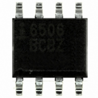
ISL6506BCBZ Intersil, ISL6506BCBZ Datasheet - Page 6

ISL6506BCBZ
Manufacturer Part Number
ISL6506BCBZ
Description
IC PWR SUPPLY CTRLR/MONITR 8SOIC
Manufacturer
Intersil
Datasheet
1.ISL6506BCBZ.pdf
(8 pages)
Specifications of ISL6506BCBZ
Applications
Power Supply Controller/Monitor
Voltage - Supply
4.75 V ~ 5.25 V
Current - Supply
3.6mA
Operating Temperature
0°C ~ 70°C
Mounting Type
Surface Mount
Package / Case
8-SOIC (3.9mm Width) Exposed Pad, 8-eSOIC. 8-HSOIC
Operating Temperature (max)
70C
Operating Temperature (min)
0C
Pin Count
8
Mounting
Surface Mount
Package Type
SOIC N EP
Screening Level
Commercial
Peak Reflow Compatible (260 C)
Yes
Rohs Compliant
Yes
Lead Free Status / RoHS Status
Lead free / RoHS Compliant
Voltage - Input
-
Lead Free Status / Rohs Status
Compliant
Available stocks
Company
Part Number
Manufacturer
Quantity
Price
Part Number:
ISL6506BCBZ
Manufacturer:
INTERSIL
Quantity:
20 000
Company:
Part Number:
ISL6506BCBZ-T
Manufacturer:
INTERSIL
Quantity:
82
Company:
Part Number:
ISL6506BCBZ-T
Manufacturer:
INSL
Quantity:
4 416
Part Number:
ISL6506BCBZ-T
Manufacturer:
INTERSIL
Quantity:
20 000
to a high impedance state, which allows the 12V rail to
enhance the two N-MOSFETs (Q
ATX rails to the 3.3V
pin is actively pulled high, which will turn the P-MOSFET
(Q
3.3V
Internal Linear Regulator Undervoltage Protection
The undervoltage protection on the internal linear regulator
is only active during sleep states and after the initial soft-start
ramp of the 3.3V linear regulator. The undervoltage trip point
is set at 25% below nominal, or 2.475V.
When an undervoltage is detected, the 3.3V linear regulator
is disabled. One soft-start interval later, the 3.3V linear
regulator is retried with a soft-start ramp. If the linear
regulator is retried 3 times and a fourth undervoltage is
detected, then the 3.3V linear regulator is disabled and can
only be reset through a POR reset.
Internal Linear Regulator Overcurrent Protection
When an overcurrent condition is detected, the gate voltage
to the internal NMOS pass element is reduced, which
causes the output voltage of the linear regulator to be
reduced. When the output voltage is reduced to the
undervoltage trip point, the undervoltage protection is
initiated and the output will shutdown.
Layout Considerations
The typical application employing an ISL6506 is a fairly
straight forward implementation. Like with any other linear
regulator, attention has to be paid to the few potentially
sensitive small signal components, such as those connected
to sensitive nodes or those supplying critical bypass current.
The power components (pass transistors) and the controller
IC should be placed first. The controller should be placed in
a central position on the motherboard, not excessively far
from the 3.3V
3V3AUX connection is properly sized to carry 1A without
exhibiting significant resistive losses at the load end.
Similarly, the input bias supply (5V
of current (for best results, ensure it is connected to its
respective source through an adequately sized trace and is
properly decoupled). The pass transistors should be placed
on pads capable of heatsinking matching the device’s power
dissipation. Where applicable, multiple via connections to a
large internal plane can significantly lower localized device
temperature rise.
Placement of the decoupling and bulk capacitors should
reflect their purpose. As such, the high-frequency
decoupling capacitors should be placed as close as possible
to the load they are decoupling; the ones decoupling the
controller close to the controller pins, the ones decoupling
the load close to the load connector or the load itself (if
embedded). Even though bulk capacitance (aluminum
electrolytics or tantalum capacitors) placement is not as
2
) off. Finally, the internal LDO which regulates the
DUAL
rail in sleep states is put in standby mode.
DUAL
island or the I/O circuitry. Ensure the
DUAL
and 5V
6
1
DUAL
SB
and Q
) carries a similar level
rails. The 5VDLSB
3
) that connect the
ISL6506, ISL6506A, ISL6506B
critical as the high-frequency capacitor placement, having
these capacitors close to the load they serve is preferable.
Locate all small signal components close to the respective
pins of the control IC, and connect them to ground, if
applicable, through a via placed close to the ground pad.
A multi-layer printed circuit board is recommended.
Figure 5 shows the connections to most of the components
in the circuit. Note that the individual capacitors shown each
could represent numerous physical capacitors. Dedicate one
solid layer for a ground plane and make all critical
component ground connections through vias placed as close
to the component terminal as possible. The EPAD should be
tied to the ground plane with three to five vias for good
thermal management. Dedicate another solid layer as a
power plane and break this plane into smaller islands of
common voltage levels. Ideally, the power plane should
support both the input power and output power nodes. Use
copper filled polygons on the top and bottom circuit layers to
create power islands connecting the filtering components
(output capacitors) and the loads. Use the remaining printed
circuit layers for small signal wiring.
Component Selection Guidelines
Output Capacitors Selection
The output capacitors should be selected to allow the output
voltage to meet the dynamic regulation requirements of
active state operation (S0/S1). The load transient for the
various microprocessor system’s components may require
high quality capacitors to supply the high slew rate (di/dt)
12VATX
+3.3VIN
Q2
FIGURE 5. PRINTED CIRCUIT BOARD ISLANDS
C
HF3V
KEY
3V3DUAL
C
5VSB
VIA CONNECTION TO GROUND PLANE
ISLAND ON POWER PLANE LAYER
ISLAND ON CIRCUIT/POWER PLANE LAYER
C
3V
VCC
3V3AUX
GND
ISL6506A,
ISL6506B
ISL6506,
5VSB
5VDLSB
EPAD
DLA
C
5V
5VDUAL
CIN
October 21, 2010
C
Q4
Q3
HF5V
5VATX
FN9141.4


