ISL6506ACBZ Intersil, ISL6506ACBZ Datasheet - Page 4
ISL6506ACBZ
Manufacturer Part Number
ISL6506ACBZ
Description
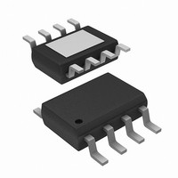
IC PWR SUPPLY CTRLR/MONITR 8SOIC
Manufacturer
Intersil
Datasheet
1.ISL6506BCBZ.pdf
(8 pages)
Specifications of ISL6506ACBZ
Applications
Power Supply Controller/Monitor
Voltage - Supply
4.75 V ~ 5.25 V
Current - Supply
3.6mA
Operating Temperature
0°C ~ 70°C
Mounting Type
Surface Mount
Package / Case
8-SOIC (3.9mm Width) Exposed Pad, 8-eSOIC. 8-HSOIC
Lead Free Status / RoHS Status
Lead free / RoHS Compliant
Voltage - Input
-
Available stocks
Company
Part Number
Manufacturer
Quantity
Price
Company:

Part Number:
ISL6506ACBZ-T
Manufacturer:
INTERSIL
Quantity:
3 213
Part Number:
ISL6506ACBZ-T
Manufacturer:
INTERSIL
Quantity:
20 000


Functional Pin Description
VCC (Pin 1)
Provide a very well decoupled 5V bias supply for the IC to
this pin by connecting it to the ATX 5V
provides all the bias for the IC as well as the input voltage for
the internal standby 3V3AUX LDO. The voltage at this pin is
monitored for power-on reset (POR) purposes.
GND (Pin 5, Pad)
Signal ground for the IC. These pins are also the ground
return for the internal 3V3AUX LDO that is active in
S3/S4/S5 sleep states. All voltage levels are measured with
respect to these pins.
S3 and S5 (Pins 3 and 4)
These pins switch the IC’s operating state from active (S0,
S1/S2) to S3 and S4/S5 sleep states. These are digital
inputs featuring internal 10µA pull-down current sources on
each pin. Additional circuitry blocks illegal state transitions,
such as S4/S5 to S3. Connect S3 and S5 to the computer
system’s SLP_S3 and SLP_S5 signals, respectively.
3V3AUX (Pin 2)
Connect this pin to the 3V3DUAL output. In sleep states, the
voltage at this pin is regulated to 3.3V through an internal
pass device powered from 5VSBY through the VCC pin. In
active states, ATX 3.3V output is delivered to this node
through a fully-on NMOS transistor. During S3 and S4/S5
states, this pin is monitored for undervoltage events.
DLA (Pin 6)
This pin is an open-drain output. A 1kΩ resistor must be
connected from this pin to the ATX 12V output. This resistor
is used to pull the gates of suitable N-MOSFETs to 12V,
which in active state, switch in the ATX 3.3V and 5V outputs
into the 3.3V
is also used to monitor the 12V rail during POR. If a resistor
other than 1kΩ is used, the POR level will be affected.
5VDLSB (Pin 7)
Connect this pin to the gate of a suitable P-MOSFET.
ISL6506 and ISL6506B: In S3 sleep state, this transistor is
switched on, connecting the ATX 5V
regulator output.
ISL6506A: In S3 and S4/S5 sleep state, this transistor is
switched on, connecting the ATX 5V
regulator output.
Description
Operation
The ISL6506 controls 2 output voltages, 3.3V
5V
applications requiring 3.3V, 5V, 5V
from an ATX power supply. The IC is composed of one linear
DUAL
. It is designed for microprocessor computer
AUX
and 5V
DUAL
4
outputs, respectively. This pin
SB
SB
SB
, and 12V bias input
SB
output to the 5V
output to the 5V
output. This pin
ISL6506, ISL6506A, ISL6506B
DUAL
and
DUAL
DUAL
controller/regulator supplying the computer system’s
3.3V
5V
functions necessary for complete ACPI implementation.
Initialization
The ISL6506 automatically initializes upon receipt of input
power. The Power-On Reset (POR) function continually
monitors the 5V
monitors the 12V rail to insure that the ATX rails are up
before entering into the S0 state even if both SLP_S3 and
SLP_S5 are both high.
Dual Outputs Operational Truth Table
Table 1 describes the truth combinations pertaining to the
3.3V
not allow the transition from an S4/S5 state to an S3 state.
NOTE: Combination Not Allowed.
Functional Timing Diagrams
Figures 1 (ISL6506, ISL6506B) and 2 (ISL6506A) are simplified
timing diagrams, detailing the power-up/down sequences of all
the outputs in response to the status of the sleep-state pins (S3,
S5), as well as the status of the input ATX supply. Not shown in
these diagrams is the deglitching feature used to protect
against false sleep state tripping. Additionally, the ISL6506
features a 60µs delay in transitioning from S0 to S3 states. The
transition from the S0 state to S4/S5 state is immediate.
3.3V, 5V, 12V
S5
5VDLSB
DUAL
1
1
0
0
0
3V3AUX
FIGURE 1. 5V
DUAL
DUAL
5VSB
5VDL
DLA
S3
S5
voltage, as well as all the control and monitoring
S3
TABLE 1. 5V
1
0
1
0
0
power, a dual switch controller supplying the
and 5V
ISL6506 AND ISL6506B
SB
3.3AUX
DUAL
DUAL
3.3V
3.3V
3.3V
3.3V
input supply voltage. The ISL6506 also
AND 3.3V
DUAL
Note
outputs. The internal circuitry does
OUTPUT TRUTH TABLE
5VDL
5V
5V
0V
5V
AUX
TIMING DIAGRAM;
S0/S1/S2 States (Active)
S3
Maintains Previous State
S4/S5 (ISL6506 and
ISL6506B)
S4/S5 (ISL6506A)
COMMENTS
October 21, 2010
FN9141.4
Related parts for ISL6506ACBZ
Image
Part Number
Description
Manufacturer
Datasheet
Request
R

Part Number:
Description:
Multiple Linear Power Controller with ACPI Control Interface
Manufacturer:
INTERSIL [Intersil Corporation]
Datasheet:

Part Number:
Description:
Intersil Corporation [CMOS Serial Controller Interface]
Manufacturer:
Intersil Corporation
Datasheet:
Part Number:
Description:
Manufacturer:
Intersil Corporation
Datasheet:
Part Number:
Description:
357-036-542-201 CARDEDGE 36POS DL .156 BLK LOPRO
Manufacturer:
Intersil Corporation
Datasheet:
Part Number:
Description:
1024-Word x 4-Bit LSI Static RAM
Manufacturer:
Intersil Corporation
Datasheet:
Part Number:
Description:
General Purpose NPN Transistor Arrays FN341.4
Manufacturer:
Intersil Corporation
Datasheet:
Part Number:
Description:
CMOS 16-Bit Microprocessor
Manufacturer:
Intersil Corporation
Datasheet:
Part Number:
Description:
Manufacturer:
Intersil Corporation
Datasheet:
Part Number:
Description:
Manufacturer:
Intersil Corporation
Datasheet:
Part Number:
Description:
Manufacturer:
Intersil Corporation
Datasheet:
Part Number:
Description:
Manufacturer:
Intersil Corporation
Datasheet:
Part Number:
Description:
CMOS 6-Bit Latch and Decoder Memory Interfaces
Manufacturer:
Intersil Corporation
Datasheet:
Part Number:
Description:
CA3046General Purpose NPN Transistor Arrays
Manufacturer:
Intersil Corporation
Datasheet:
Part Number:
Description:
Manufacturer:
Intersil Corporation
Datasheet:
Part Number:
Description:
TR909 DLC/FLC SLIC with Low Power Standby
Manufacturer:
Intersil Corporation
Datasheet: