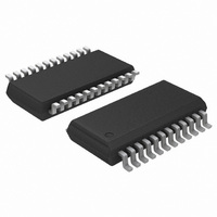
ADT7476ARQZ ON Semiconductor, ADT7476ARQZ Datasheet - Page 10

ADT7476ARQZ
Manufacturer Part Number
ADT7476ARQZ
Description
IC REMOTE THERMAL CTRLR 24QSOP
Manufacturer
ON Semiconductor
Series
dBCool®r
Datasheet
1.ADT7476ARQZ-REEL.pdf
(67 pages)
Specifications of ADT7476ARQZ
Function
Fan Control, Temp Monitor
Topology
ADC, Comparator, Fan Speed Counter, Multiplexer, Register Bank
Sensor Type
External & Internal
Sensing Temperature
-40°C ~ 125°C, External Sensor
Output Type
SMBus™
Output Alarm
No
Output Fan
Yes
Voltage - Supply
3 V ~ 3.6 V
Operating Temperature
-40°C ~ 125°C
Mounting Type
Surface Mount
Package / Case
24-QSOP
Full Temp Accuracy
+/- 0.5 C
Digital Output - Bus Interface
Serial (3-Wire, 4-Wire)
Maximum Operating Temperature
+ 125 C
Minimum Operating Temperature
- 40 C
Lead Free Status / RoHS Status
Lead free / RoHS Compliant
Available stocks
Company
Part Number
Manufacturer
Quantity
Price
Part Number:
ADT7476ARQZ
Manufacturer:
ADI/亚德诺
Quantity:
20 000
Part Number:
ADT7476ARQZ-REEL
Manufacturer:
ON/安森美
Quantity:
20 000
Company:
Part Number:
ADT7476ARQZ-REEL7
Manufacturer:
ON
Quantity:
6 028
Serial Bus Interface
system management bus (SMBus). The ADT7476 is
connected to this bus as a slave device, under the control of
a master controller. The ADT7476 has a 7−bit serial bus
address. When the device is powered up with Pin 13
(PWM3/ADDREN) high, the ADT7476 has a default
SMBus address of 0101110 or 0x2E. The read/write bit must
be added to get the 8−bit address. If more than one ADT7476
is to be used in a system, each ADT7476 is placed in ADDR
SELECT mode by strapping Pin 13 low on powerup. The
logic state of Pin 14 then determines the device’s SMBus
address. The logic of these pins is sampled on powerup.
the first valid SMBus transaction, more precisely on the
low−to−high transition at the beginning of the eighth SCL
pulse, when the serial bus address byte matches the selected
slave address. The selected slave address is chosen using the
ADDREN pin/ADDR SELECT pin. Any attempted
changes in the address have no effect after this.
Table 1. Hardwiring the ADT7476 SMBus Device
Address
Pin 13 State
Control of the ADT7476 is carried out using the serial
The device address is sampled on powerup and latched on
Figure 15. SMBus Address = 0x2C (Pin 14 = 0)
Figure 16. SMBus Address = 0x2D (Pin 14 = 1)
Figure 14. Default SMBus Address = 0x2E
0
0
1
PWM3/ADDREN
PWM3/ADDREN
PWM3/ADDREN
Low (10 kW to GND)
High (10 kW pullup)
Don’t care
ADDR SELECT
ADDR SELECT
ADDR SELECT
ADT7476
ADT7476
ADT7476
Pin 14 State
14
13
ADDRESS = 0x2D
14
13
ADDRESS = 0x2E
14
13
ADDRESS = 0x2C
V
10k
V
CC
CC
10k
10kW
W
W
0101100 (0x2C)
0101101 (0x2D)
0101110 (0x2E)
Address
http://onsemi.com
10
slave address allows the user to avoid conflicts with other
devices sharing the same serial bus, for example, if more
than one ADT7476 is used in a system.
The serial bus protocol operates as follows:
The ability to make hardwired changes to the SMBus
Figure 17. Unpredictable SMBus Address if Pin 13
1. The master initiates data transfer by establishing a
2. Data is sent over the serial bus in sequences of nine
3. When all data bytes have been read or written, stop
CARE SHOULD BE TAKEN TO ENSURE THAT PIN 13
(PWM3/ADDREN) IS EITHER TIED HIGH OR LOW. LEAVING PIN 13
FLOATING COULD CAUSE THE ADT7476 TO POWER UP WITH AN
UNEXPECTED ADDRESS.
NOTE THAT IF THE ADT7476 IS PLACED INTO ADDR SELECT
MODE, PINS 13 AND 14 CANNOT BE USED AS THE ALTERNATIVE
FUNCTIONS (PWM3, TACH4/THERM) UNLESS THE CORRECT
CIRCUIT IS MUXED IN AT THE CORRECT TIME OR DESIGNED TO
HANDLE THESE DUAL FUNCTIONS.
start condition, which is defined as a high−to−low
transition on the serial data line SDA while the
serial clock line SCL remains high. This indicates
that an address/data stream follows. All slave
peripherals connected to the serial bus respond to
the start condition and shift in the next eight bits,
consisting of a 7−bit address (MSB first), plus a
R/W bit, which determine the direction of the data
transfer, that is, whether data is written to or read
from the slave device.
The peripheral whose address corresponds to the
transmitted address responds by pulling the data
line low during the low period before the ninth
clock pulse, known as the acknowledge bit. All
other devices on the bus now remain idle while the
selected device waits for data to be read from or
written to it. If the R/W bit is a 0, the master writes
to the slave device. If the R/W bit is a 1, the master
reads from the slave device.
clock pulses, eight bits of data followed by an
acknowledge bit from the slave device. Transitions
on the data line must occur during the low period of
the clock signal and remain stable during the high
period. A low−to−high transition, when the clock is
high, can be interpreted as a stop signal. The
number of data bytes transmitted over the serial bus
in a single read or write operation is limited only by
what the master and slave devices can handle.
conditions are established. In write mode, the
master pulls the data line high during the 10
PWM3/ADDREN
ADDR SELECT
ADT7476
is Unconnected
14
13
DO NOT LEAVE ADDREN
UNCONNECTED! CAN
CAUSE UNPREDICTABLE
ADDRESSES.
V
CC
NC
10k
W
th
clock


