ADT7476ARQZ ON Semiconductor, ADT7476ARQZ Datasheet - Page 16
ADT7476ARQZ
Manufacturer Part Number
ADT7476ARQZ
Description
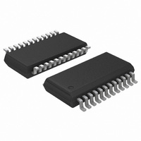
IC REMOTE THERMAL CTRLR 24QSOP
Manufacturer
ON Semiconductor
Series
dBCool®r
Datasheet
1.ADT7476ARQZ-REEL.pdf
(67 pages)
Specifications of ADT7476ARQZ
Function
Fan Control, Temp Monitor
Topology
ADC, Comparator, Fan Speed Counter, Multiplexer, Register Bank
Sensor Type
External & Internal
Sensing Temperature
-40°C ~ 125°C, External Sensor
Output Type
SMBus™
Output Alarm
No
Output Fan
Yes
Voltage - Supply
3 V ~ 3.6 V
Operating Temperature
-40°C ~ 125°C
Mounting Type
Surface Mount
Package / Case
24-QSOP
Full Temp Accuracy
+/- 0.5 C
Digital Output - Bus Interface
Serial (3-Wire, 4-Wire)
Maximum Operating Temperature
+ 125 C
Minimum Operating Temperature
- 40 C
Lead Free Status / RoHS Status
Lead free / RoHS Compliant
Available stocks
Company
Part Number
Manufacturer
Quantity
Price

Part Number:
ADT7476ARQZ
Manufacturer:
ADI/亚德诺
Quantity:
20 000
Part Number:
ADT7476ARQZ-REEL
Manufacturer:
ON/安森美
Quantity:
20 000
Company:
Part Number:
ADT7476ARQZ-REEL7
Manufacturer:
ON
Quantity:
6 028


VID Code Monitoring
inputs. These are digital inputs that can be read back through
the VID/GPIO register (0x43) to determine the processor
voltage required or the system being used. Five VID code
inputs support VRM9.x solutions. In addition, Pin 21 (12 V
input) can be reconfigured as a sixth VID input to satisfy
future VRM requirements.
VID/GPIO Register (0x43)
[0] = VID0, reflects logic state of Pin 5.
[1] = VID1, reflects logic state of Pin 6.
[2] = VID2, reflects logic state of Pin 7.
[3] = VID3, reflects logic state of Pin 8.
[4] = VID4, reflects logic state of Pin 19.
[5] = VID5, reconfigurable 12 V input. This bit reads 0 when
Pin 21 is configured as the 12 V input. This bit reflects the
logic state of Pin 21 when the pin is configured as VID5.
VID Code Input Threshold Voltage
approximately 1.0 V. To enable future compatibility, it is
possible to reduce the VID code input threshold to 0.6 V.
Bit 6 (THLD) of the VID/GPIO register (0x43) controls the
VID input threshold voltage.
VID/GPIO Register (0x43)
[6] THLD = 0, VID switching threshold = 1.0 V,
V
[6] THLD = 1, VID switching threshold = 0.6 V,
V
Reconfiguring Pin 21 as VID5 Input
(VID5) for VRM10 compatible systems. Because the pin is
configured as VID5, it is not possible to monitor a 12 V
supply.
function of Pin 21. System or BIOS software can read the
state of Bit 7 to determine whether the system is designed to
monitor 12 V or a sixth VID input.
VID/GPIO Register (0x43)
[7] VIDSEL = 0, Pin 21 functions as a 12 V measurement
input. Software can read this bit to determine that there are
five VID inputs being monitored. Bit 5 of VID/GPIO
Register (0x43) always reads back 0. Bit 0 of Interrupt Status
Register 2 (0x42) reflects 12 V out−of−limit measurements.
[7] VIDSEL = 1, Pin 21 functions as the sixth VID code
input (VID5). Software can read this bit to determine that
there are six VID inputs being monitored. Bit 5 of Register
0x43 reflects the logic state of Pin 21. Bit 0 of Interrupt
Status Register 2 (0x42) reflects VID code changes.
OL
OL
The ADT7476 has five dedicated voltage ID (VID code)
The switching threshold for the VID code inputs is
Pin 21 can be reconfigured as a sixth VID code input
Bit 7 of the VID/GPIO register (0x43) determines the
< 0.8 V, V
< 0.4 V, V
IH
IH
> 1.7 V, V
> 0.8 V, V
MAX
MAX
= 3.3 V.
= 3.3 V.
http://onsemi.com
16
VID Code Change Detect Function
When Pin 21 is configured as the VID5 input, VID code
changes are detected and reported back by the ADT7476. Bit
0 of Interrupt Status Register 2 (0x42) is the 12 V/VC bit and
denotes a VID change when set. The VID code change bit is
set when the logic states on the VID inputs are different than
they were 11 ms previously. The change of VID code is used
to generate an SMBALERT interrupt. If an SMBALERT
interrupt is not required, Bit 0 of Interrupt Mask Register 2
(0x75), when set, prevents SMBALERTs from occurring on
VID code changes.
Interrupt Status Register 2 (0x42)
[0] 12 V/VC = 0, if Pin 21 is configured as VID5, Logic 0
denotes no change in VID code within the last 11 ms.
[0] 12 V/VC = 1, if Pin 21 is configured as VID5, Logic 1
means that a change has occurred on the VID code inputs
within the last 11 ms. An SMBALERT is generated, if this
function is enabled.
Programming the GPIOs
to the ADT7476. In order to maintain consistency between
versions, it is necessary to omit references to GPIO5. As a
result, there are six GPIOs as follows: GPIO0, GPIO1, GPIO2,
GPIO3, GPIO4, and GPIO6.
enables GPIO functionality. This turns all pins configured as
VID inputs into general−purpose outputs. Writing to the
corresponding VID bit in the VID/GPIO register (0x43) sets
the polarity for the corresponding GPIO. GPIO6 can be
programmed independently as, for example, an input or
output, using Bits [3:2] of Configuration Register 5 (0x7C).
Temperature Measurement Method
Local Temperature Measurement
sensor whose output is digitized by the on−chip, 10−bit
ADC. The 8−bit MSB temperature data is stored in the
temperature registers (Addresses 0x25, 0x26, and 0x27).
Because both positive and negative temperatures can be
measured, the temperature data is stored in Offset 64 format
or twos complement format, as shown in Table 6 and
Table 7. Theoretically, the temperature sensor and ADC can
measure temperatures from −63°C to +127°C (or −61°C to
+191°C in the extended temperature range) with a resolution
of 0.25°C. However, this exceeds the operating temperature
range of the device, so local temperature measurements
outside the ADT7476 operating temperature range are not
possible.
The ADT7476 has a VID code change detect function.
The ADT7476 follows an upgrade path from the ADM1027
Setting Bit 4 of Configuration Register 5 (0x7C) to 1
The ADT7476 contains an on−chip band gap temperature
Related parts for ADT7476ARQZ
Image
Part Number
Description
Manufacturer
Datasheet
Request
R

Part Number:
Description:
ON Semiconductor [VOLTAGE REGULATOR]
Manufacturer:
ON Semiconductor
Datasheet:
Part Number:
Description:
357-036-542-201 CARDEDGE 36POS DL .156 BLK LOPRO
Manufacturer:
ON Semiconductor
Datasheet:
Part Number:
Description:
357-036-542-201 CARDEDGE 36POS DL .156 BLK LOPRO
Manufacturer:
ON Semiconductor
Datasheet:
Part Number:
Description:
357-036-542-201 CARDEDGE 36POS DL .156 BLK LOPRO
Manufacturer:
ON Semiconductor
Datasheet:
Part Number:
Description:
357-036-542-201 CARDEDGE 36POS DL .156 BLK LOPRO
Manufacturer:
ON Semiconductor
Datasheet:
Part Number:
Description:
357-036-542-201 CARDEDGE 36POS DL .156 BLK LOPRO
Manufacturer:
ON Semiconductor
Datasheet:
Part Number:
Description:
357-036-542-201 CARDEDGE 36POS DL .156 BLK LOPRO
Manufacturer:
ON Semiconductor
Datasheet:
Part Number:
Description:
357-036-542-201 CARDEDGE 36POS DL .156 BLK LOPRO
Manufacturer:
ON Semiconductor
Datasheet:
Part Number:
Description:
357-036-542-201 CARDEDGE 36POS DL .156 BLK LOPRO
Manufacturer:
ON Semiconductor
Datasheet:
Part Number:
Description:
357-036-542-201 CARDEDGE 36POS DL .156 BLK LOPRO
Manufacturer:
ON Semiconductor
Datasheet:
Part Number:
Description:
357-036-542-201 CARDEDGE 36POS DL .156 BLK LOPRO
Manufacturer:
ON Semiconductor
Datasheet:
Part Number:
Description:
Manufacturer:
ON Semiconductor
Datasheet:
Part Number:
Description:
Manufacturer:
ON Semiconductor
Datasheet:
Part Number:
Description:
Manufacturer:
ON Semiconductor
Datasheet: