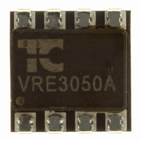
VRE3050AS Cirrus Logic Inc, VRE3050AS Datasheet - Page 2

VRE3050AS
Manufacturer Part Number
VRE3050AS
Description
IC VOLT REF PREC 5V 8-SMD
Manufacturer
Cirrus Logic Inc
Datasheet
1.VRE3050BS.pdf
(6 pages)
Specifications of VRE3050AS
Reference Type
Series
Voltage - Output
5V
Tolerance
±0.5mV
Temperature Coefficient
0.6ppm/°C
Voltage - Input
8 ~ 36 V
Number Of Channels
1
Current - Quiescent
4mA
Current - Output
15mA
Operating Temperature
0°C ~ 70°C
Mounting Type
Surface Mount
Package / Case
8-SMD
Product
Voltage References
Topology
Series References
Output Voltage
5 V
Average Temperature Coefficient (typ)
0.6 PPM / C
Series Vref - Input Voltage (max)
40 V
Shunt Current (max)
15 mA
Maximum Operating Temperature
+ 70 C
Minimum Operating Temperature
0 C
Mounting Style
SMD/SMT
Lead Free Status / RoHS Status
Lead free / RoHS Compliant
Current - Cathode
-
Lead Free Status / Rohs Status
Lead free / RoHS Compliant
Other names
598-1774
VRE3050
1. CHARACTERISTICS AND SPECIFICATIONS
ABSOLUTE MAXIMUM RATINGS
Power Supply ........................... -0.3V to +40V
OUT, TRIM ................................ -0.3V to +12V
NR .............................................. -0.3V to +6V
Operating Temp. (A,B,C) ........... 0ºC to +70ºC
Operating Temp. (J,K,L) ......... -40ºC to +85ºC
ELECTRICAL SPECIFICATIONS
V
NOTES:
2
Input Voltage
Output Voltage (Note 1)
Output Voltage
Temperature Coefficient
(Note 2)
Trim Adjustment Range
Turn-On Settling Time
Output Noise Voltage
Temperature Hysterisis
Long Term Stability
Supply Current
Load Regualtion (Note 3) ∆V
Line Regulation
PS
=+15V, T = +25ºC, R
Parameter
1. The specified values are without external trim.
2. The temperature coefficient is determined by the box method. See discussion on temperature perfor-
3. Line and load regulation are measured with pulses and do not include voltage changes due to tem-
4. Hysterisis over the operating temperature range.
mance.
perature.
(Note 3)
L
= 10KΩ Unless Otherwise Noted.
∆V
Symbol
TCV
∆V
OUT
∆V
OUT
V
T
V
e
I
OUT
ON
OUT/t
IN
/ ∆I
IN
OUT
/ ∆V
n
OUT
OUT
IN
Sourcing: 0mA ≤ I
Sinking: -15mA ≤ I
To 0.01% of final value
0.1Hz < f < 10Hz
10Hz < f < 1kHz
10V ≤ V
8V ≤ V
VRE3050B/K
VRE3050C/L
VRE3050B/K
VRE3050C/L
VRE3050A/J
VRE3050A/J
Conditions
Figure 3
Note 4
Out Short Circuit to GND Duration (V
Out Short Circuit to GND Duration (V
Out Short Circuit to IN Duration (V
Continuous Power Dissipation (T
Storage Temperature ......................................... -65ºC to +150ºC
Lead Temperature (soldering,10 sec) .............................. +250ºC
®
IN
IN
P r o d u c t I n n o v a t i o n F r o m
≤ 10V
≤ 18V
OUT
OUT
≤ 15mA
≤ 0mA
+4.9995
+4.9992
+4.9990
Min
+8
+5.0000
+5.0000
+5.0000
±5.0
Typ
0.3
0.5
1.0
2.0
3.0
2.5
3.5
25
1
6
8
8
5
A
IN
= +70ºC) .................... 300mW
< 12V) ............... Continuous
IN
IN
< 12V) ........... Continuous
< 40V) .....................5 sec
+5.0005
+5.0008
+5.0010
Max
+36
0.6
1.0
2.0
5.0
4.0
12
12
35
10
ppm/1000hrs.
VRE3050DS
ppm/mA
ppm/ºC
ppm/V
µVp-p
Units
µV
ppm
mV
mA
µs
V
V
RMS


