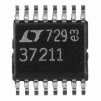
LTC3721EGN-1#PBF Linear Technology, LTC3721EGN-1#PBF Datasheet

LTC3721EGN-1#PBF
Specifications of LTC3721EGN-1#PBF
Available stocks
Related parts for LTC3721EGN-1#PBF
LTC3721EGN-1#PBF Summary of contents
Page 1
... The LTC3721-1 features extremely low operating and start-up currents and reliable short-circuit and overtemperature protection. The LTC3721-1 is offered in 16-pin SSOP and (4mm × 4mm) QFN packages. , LTC and LT are registered trademarks of Linear Technology Corporation. Isolated Push-Pull Converter UVLO DRVA DRVB ...
Page 2
... Output Current ............................... Self-Regulated REF Operating Temperature (Notes 5,6) LTC3721-1 ......................................... – 40°C to 85°C CC Storage Temperature Range ................. – 65°C to 125°C Lead Temperature (GN Package only) (Soldering, 10sec) ............................................ 300° ORDER PART TOP VIEW NUMBER 16 LTC3721EGN-1 DRVB DRVA 3 PGND 4 GN PART 5 MARKING 37211 UF PACKAGE 16-LEAD (4mm × ...
Page 3
ELECTRICAL CHARACTERISTICS temperature range, otherwise specifications are at T SYMBOL PARAMETER Pulse Width Modulator ROS Ramp Offset Voltage I Ramp Discharge Current RMP I Slope Compensation Current SLP DCMAX Maximum Duty Cycle DCMIN Minimum Duty Cycle DTADJ Dead-Time Oscillator OSCI ...
Page 4
LTC3721-1 ELECTRICAL CHARACTERISTICS temperature range, otherwise specifications are at T SYMBOL PARAMETER SSR Soft-Start Reset Threshold FLT Fault Reset Threshold Note 1: Absolute Maximum Ratings are those values beyond which the life of a device may be impaired. Note 2: ...
Page 5
W U TYPICAL PERFOR A CE CHARACTERISTICS Error Amplifier Gain/Phase 100 –180 –270 –360 10 100 1k 10k 100k 1M FREQUENCY (Hz) 372311 G07 Slope Current vs Temperature 2.25V T 70 ...
Page 6
LTC3721 DESCRIPTIO S (GN Package/UF Package) V (Pin 1/Pin 15): Output of the 5.0V Reference. V REF capable of supplying up to 18mA to external circuitry. V should be decoupled to GND with a 1µF ceramic capacitor. ...
Page 7
DESCRIPTIO S (GN Package/UF Package) FB (Pin 13/Pin 12): Error Amplifier Inverting Input. This is the voltage feedback input for the LTC3721-1. The nomi- nal regulation voltage 1.2V. SS (Pin 14/Pin 13): Soft-Start/Restart Delay ...
Page 8
LTC3721-1 W BLOCK DIAGRA S 8 sn37211 37211fs ...
Page 9
U OPERATIO Please refer to the detailed Block Diagram for this discus- sion. The LTC3721 PWM push-pull controller that operates with pulse-by-pulse peak current mode control best suited for moderate to high power isolated power systems ...
Page 10
LTC3721-1 U OPERATIO V should be bypassed with a 0.1µF to 1µF multilayer CC ceramic capacitor to decouple the fast transient currents demanded by the output drivers and a bulk tantalum or electrolytic capacitor to hold up the V bootstrap ...
Page 11
U OPERATIO that the positive voltage square wave is produced while the output inductor is freewheeling. An advantage of this technique over the previous is that it does not require a separate filter inductor and since the voltage is derived ...
Page 12
LTC3721-1 U OPERATIO Leading Edge Blanking The LTC3721-1 provides programmable leading edge blanking to prevent nuisance tripping of the current sense circuitry. Leading edge blanking relieves the filtering re- quirements for the CS pin, greatly improving the response to real ...
Page 13
U OPERATIO The duty cycle of these square waves is guaranteed to never exceed 50% by the LTC3721-1. In steady state operation, the duty ratio is given by /(2 • V • N) OUT IN To calculate ...
Page 14
LTC3721-1 PACKAGE DESCRIPTIO .254 MIN .0165 ± .0015 RECOMMENDED SOLDER PAD LAYOUT .007 – .0098 (0.178 – 0.249) .016 – .050 (0.406 – 1.270) NOTE: 1. CONTROLLING DIMENSION: INCHES INCHES 2. DIMENSIONS ARE IN (MILLIMETERS) 3. DRAWING NOT TO SCALE ...
Page 15
... SHADED AREA IS ONLY A REFERENCE FOR PIN 1 LOCATION ON THE TOP AND BOTTOM OF PACKAGE Information furnished by Linear Technology Corporation is believed to be accurate and reliable. However, no responsibility is assumed for its use. Linear Technology Corporation makes no represen- tation that the interconnection of its circuits as described herein will not infringe on existing patent rights Package 16-Lead Plastic QFN (4mm × ...
Page 16
... IN 2xSi7370DP –V IN 1.21k 5V 73.2k 4.7Ω 1/4W 330pF FMMT718 FMMT718 V IN 470Ω MMBT3904LT1 6 10 DRVA CS 470Ω 107k LTC3721EGN-1 15 UVLO C R GND LEB 1nF 1µF D1 9.1V 270pF 33k 100k RELATED PARTS PART NUMBER DESCRIPTION LT1431 Reference and Opto-Driver ...


