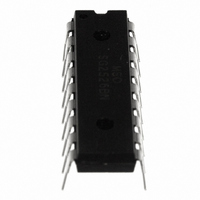
SG2526BN Microsemi Analog Mixed Signal Group, SG2526BN Datasheet

SG2526BN
Specifications of SG2526BN
SG2526BNR
Available stocks
Related parts for SG2526BN
SG2526BN Summary of contents
Page 1
DESCRIPTION The SG1526B is a high-performance pulse width modulator for switching power supplies which offers improved functional and electrical characteris- tics over the industry-standard SG1526. A direct pin-for-pin replacement for the earlier device with all its features, it incorporates the ...
Page 2
ABSOLUTE MAXIMUM RATINGS Input Voltage (V ) ............................................................... IN Collector Supply Voltage (V ) ............................................. C Logic Inputs ......................................................... Analog Inputs .......................................................... Source/Sink Load Current (each output) ....................... Reference Load Current .................................................. Note 1. Exceeding these ratings could cause damage ...
Page 3
ELECTRICAL CHARACTERISTICS Parameter Oscillator Section (Note 4) Initial Accuracy Voltage Stability Temperature Stability (Note 9) Minimum Frequency (Note 9) Maximum Frequency Sawtooth Peak Voltage Sawtooth Valley Voltage SYNC Pulse Width Error Amplifier Section (Note 5) Input Offset Voltage Input Bias ...
Page 4
CHARACTERISTIC CURVES FIGURE 1. REFERENCE VOLTAGE VS. SUPPLY VOLTAGE FIGURE 4. REFERENCE RIPPLE REJECTION FIGURE 7. SOFTSTART TIME CONSTANT VS Rev 1.1a Copyright 1994 SG1526B/SG2526B/SG3526B FIGURE 2. REFERENCE TEMPERATURE STABILITY FIGURE 5. UNDER VOLTAGE LOCKOUT FIGURE 8. CURRENT ...
Page 5
CHARACTERISTIC CURVES (continued) FIGURE 10. STANDBY CURRENT VS. SUPPLY VOLTAGE FIGURE 13. SUPPLY CURRENT VS. OUTPUT FREQUENCY FIGURE 16. OSCILLATOR FREQUENCY TEMPERATURE STABILITY Rev 1.1a Copyright 1994 SG1526B/SG2526B/SG3526B FIGURE 11. OUTPUT DRIVER DEADTIME VS. C VALUE T FIGURE 14. SUPPLY ...
Page 6
CHARACTERISTIC CURVES FIGURE 19. OSCILLATOR PERIOD VS. R AND APPLICATION INFORMATION VOLTAGE REFERENCE The reference regulator of the SG1526B is a “band-gap” type; that is, the precision +5 volt output is derived from the very predictable base-emitter ...
Page 7
APPLICATION INFORMATION DIGITAL CONTROL PORTS The three digital control ports of the SG1526B are bi- directional. Each pin can drive TTL and 5 volt CMOS logic directly fan-out of 10 low-power Schottky gates. Each pin can also ...
Page 8
APPLICATION INFORMATION OUTPUT DRIVERS The totem-pole output drivers of the SG1526B are designed to source and sink 100mA continuously and 200mA peak. Loads can be driven either from the output pins 13 and 16, FIGURE 26. PUSH-PULL CONFIGURATION SG1526B LAB ...
Page 9
... CONNECTION DIAGRAMS & ORDERING INFORMATION Package Part No. 18-PIN CERAMIC DIP SG1526BJ/883B J - PACKAGE JAN1526BJ SG1526BJ/DESC SG1526BJ SG2526BJ SG3526BJ 18-PIN PLASTIC DIP SG2526BN N - PACKAGE SG3526BN 18-PIN WIDE BODY SG2526BDW PLASTIC S.O.I.C. SG3526BDW DW - PACKAGE SG1526BL/883B 20-PIN CERAMIC LEADLESS CHIP CARRIER SG1526BL L- PACKAGE Note 1. Contact factory for JAN and DESC product availability. ...


