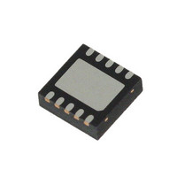
L6728AHTR STMicroelectronics, L6728AHTR Datasheet - Page 16

L6728AHTR
Manufacturer Part Number
L6728AHTR
Description
IC CTLR PWM SGL PHASE 10-VFQFPN
Manufacturer
STMicroelectronics
Datasheet
1.L6728AHTR.pdf
(33 pages)
Specifications of L6728AHTR
Pwm Type
Voltage Mode
Number Of Outputs
1
Frequency - Max
660kHz
Duty Cycle
67%
Voltage - Supply
5 V ~ 12 V
Buck
Yes
Boost
No
Flyback
No
Inverting
No
Doubler
No
Divider
No
Cuk
No
Isolated
No
Operating Temperature
-40°C ~ 125°C
Package / Case
10-VFQFN, 10-VFQFPN
Frequency-max
660kHz
Lead Free Status / RoHS Status
Lead free / RoHS Compliant
Other names
497-8977-2
Available stocks
Company
Part Number
Manufacturer
Quantity
Price
Company:
Part Number:
L6728AHTR
Manufacturer:
PHI
Quantity:
1 800
Company:
Part Number:
L6728AHTR
Manufacturer:
STMicroelectronics
Quantity:
10 000
Part Number:
L6728AHTR
Manufacturer:
ST
Quantity:
20 000
Application details
9.2
16/33
Layout guidelines
L6728AH provides control functions and high current integrated drivers to implement high-
current step-down DC-DC converters. In this kind of application, a good layout is very
important.
The first priority when placing components for these applications has to be reserved to the
power section, minimizing the length of each connection and loop as much as possible. To
minimize noise and voltage spikes (EMI and losses) power connections (highlighted in
Figure
traces: loop must be anyway minimized. The critical components, i.e. the power MOSFETs,
must be close one to the other. The use of multi-layer printed circuit board is recommended.
The input capacitance (C
placed close to the power section in order to eliminate the stray inductance generated by the
copper traces. Low ESR and ESL capacitors are preferred, MLCC are suggested to be
connected near the HS drain.
Use proper VIAs number when power traces have to move between different planes on the
PCB in order to reduce both parasitic resistance and inductance. Moreover, reproducing the
same high-current trace on more than one PCB layer will reduce the parasitic resistance
associated to that connection.
Connect output bulk capacitors (C
inductance and resistance associated to the copper trace, also adding extra decoupling
capacitors along the way to the load when this results in being far from the bulk capacitors
bank.
b)
c)
d)
e)
f)
7) must be a part of a power plane and anyway realized by wide and thick copper
Place F
Place F
Place F
Check that compensation network gain is lower than open loop EA gain before
F
Check phase margin obtained (it should be greater than 45°) and repeat if
necessary.
C
R
C
C
0dB
P
S
S
F
=
=
=
=
;
----------------------------------------------------------
2π R
-------------------------- -
----------------- - 1
2 F
------------------------------ -
π R
-----------------------------
π R
F
Z1
P1
Z2
⋅
⋅
⋅
SW
⋅
R
LC
S
below F
at F
at F
FB
F
1
1
F
⋅
⋅
–
F
⋅
F
C
SW
LC
ESR
LC
C
F
IN
F
⋅
), or at least a portion of the total capacitance needed, has to be
and F
F
:
LC
ESR
Doc ID 15726 Rev 1
(typically 0.5*F
P2
–
OUT
1
at half of the switching frequency:
) as near as possible to the load, minimizing parasitic
LC
):
L6728AH


