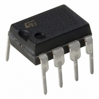
UC3844BN STMicroelectronics, UC3844BN Datasheet

UC3844BN
Specifications of UC3844BN
UC3844BNST
UC3844BNST
Available stocks
Related parts for UC3844BN
UC3844BN Summary of contents
Page 1
HIGH PERFORMANCE CURRENT MODE PWM CONTROLLER . TRIMMED OSCILLATOR FOR PRECISE FRE- . QUENCY CONTROL OSCILLATOR FREQUENCY GUARANTEED . AT 250kHz . CURRENT MODE OPERATION TO 500kHz AUTOMATIC FEED FORWARD COMPENSA- . TION LATCHING PWM FOR CYCLE-BY-CYCLE . CURRENT ...
Page 2
... D95IN332 Description to Vref and cpacitor C to ground. Operation to 500kHz is possible. T Value 30 Self Limiting 1 5 – 0.3 to 5.5 10 1.25 800 – 150 – 150 300 V REF Vi OUTPUT GROUND through resistor R T Minidip UC2842BN; UC3842BN UC2843BN; UC3843BN UC2844BN; UC3844BN UC2845BN; UC3845BN Unit ° ...
Page 3
THERMAL DATA Symbol R Thermal Resistance Junction-ambient. th j-amb ELECTRICAL CHARACTERISTICS ( [note 1] Unless otherwise stated, these specifications apply for -25 < T < for UC284XB; 0 < T amb Symbol Parameter REFERENCE SECTION V Output Voltage ...
Page 4
UC2842B/3B/4B/5B - UC3842B/3B/4B/5B ELECTRICAL CHARACTERISTICS (continued) Symbol Parameter OUTPUT SECTION V Output Low Level OL V Output High Level OH V UVLO Saturation OLS t Rise Time r t Fall Time f UNDER-VOLTAGE LOCKOUT SECTION Start Threshold Min Operating Voltage ...
Page 5
Figure 1: Open Loop Test Circuit. 4.7K 2N2222 100K ERROR AMP. ADJUST 1K I 4.7K SENSE ADJUST 5K D95IN343 High peak currents associated with capacitive loads necessitate careful grounding techniques. Timing and bypass capacitors should be connected close Figure 2: ...
Page 6
UC2842B/3B/4B/5B - UC3842B/3B/4B/5B Figure 4: Oscillator Discharge Current vs. Tem- perature. I dischg (mA 8.5 8.0 7.5 7.0 -55 - Figure 6: Error Amp Open-Loop Gain and Phase vs. Frequency. (dB) V =15V i V ...
Page 7
Figure 10: Output Saturation Voltagevs. Load Current. V sat (V) Source Saturation V i (Load to Ground =25˚ =15V Pulsed Load 120Hz Rate 3 T =-40˚ Sink Saturation (Load ...
Page 8
UC2842B/3B/4B/5B - UC3842B/3B/4B/5B Figure 15 : Error Amp Configuration Figure 16 : Under Voltage Lockout. 7 ON/OFF COMMAND OFF Figure 17 : Current Sense Circuit . CURRENT ...
Page 9
Figure 18 : Slope Compensation Techniques. V REG SLOPE SENSE R S Figure 19 : Isolated MOSFET Drive and Current Transformer Sensing ...
Page 10
UC2842B/3B/4B/5B - UC3842B/3B/4B/5B Figure 20 : Latched Shutdown. 2N 3905 SCR must be selected for a holding current of less than 0.5mA at T The simple two transistor circuit can be used in place of the SCR as shown. All ...
Page 11
Figure 22: External Clock Synchronization. EXTERNAL SYNC INPUT 0.01 F The diode clamp is required if the Sync amplitude is large enough to cause the bottom side of C Figure 23: External Duty Cycle Clamp and Multi Unit Synchronization. V ...
Page 12
UC2842B/3B/4B/5B - UC3842B/3B/4B/5B Figure 24: Soft-Start Circuit Figure 25: Soft-Start and Error Amplifier Output Duty Cycle Clamp BC109 V CLAMP 12/15 R BIAS R ...
Page 13
DIM. MIN. TYP. MAX. MIN. A 1.75 a1 0.1 0.25 0.004 a2 1.65 a3 0.65 0.85 0.026 b 0.35 0.48 0.014 b1 0.19 0.25 0.007 C 0.25 0.5 0.010 c1 45 (typ.) D (1) 4.8 5.0 0.189 E 5.8 ...
Page 14
UC2842B/3B/4B/5B - UC3842B/3B/4B/5B mm DIM. MIN. TYP. MAX. A 3.32 a1 0.51 0.020 B 1.15 1.65 0.045 b 0.356 0.55 0.014 b1 0.204 0.304 0.008 D 10.92 E 7.95 9.75 0.313 e 2.54 e3 7.62 e4 7.62 F 6.6 I ...
Page 15
... No license is granted by implication or otherwise under any patent or patent rights of STMicroelectronics. Specification mentioned in this publication are subject to change without notice. This publication supersedes and replaces all information previously supplied. STMi- croelectronics products are not authorized for use as critical components in life support devices or systems without express written approval of STMicroelectronics ...


