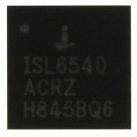
ISL6540ACRZ-T Intersil, ISL6540ACRZ-T Datasheet

ISL6540ACRZ-T
Specifications of ISL6540ACRZ-T
Related parts for ISL6540ACRZ-T
ISL6540ACRZ-T Summary of contents
Page 1
... Low-Voltage and High Current Distributed Power Supplies 22 Ordering Information 21 BOOT PART NUMBER* 20 UGATE (Note) 19 PHASE ISL6540ACRZ* ISL6540 ACRZ PGND 18 ISL6540AIRZ* 17 LGATE ISL6540AIRZA* ISL6540 AIRZ PVCC 16 *Add “-T” suffix for tape and reel. Please refer to TB347 for details on reel specifications. LINDRV ...
Page 2
Block Diagram REFIN REFOUT MAR_CTRL OFS+ VOLTAGE MARGINING OFS- OTA SS FB COMP VCC 1.8V PGOOD COMP VSEN+ VSEN UNITY GAIN DIFF AMP VMON PG_DLY EN VCC POWER-ON REFERENCE RESET (POR 0.591 V REF SOFT-START ...
Page 3
Typical Application I (Internal Linear Regulator with Remote Sense VIN * C F1 VIN INTERNAL 5.6V BIAS R VFF LINEAR REGULATOR VFF VFF EN VCC REFIN REFOUT PG C PG_DLY PG_DLY ...
Page 4
Typical Application II (External Linear Regulator without Remote Sense DRV VIN LINDRV VIN VFF VFF C VFF REFOUT VCC REFIN 1kΩ PG_DLY PG_DLY ...
Page 5
Typical Application III (Dual Data Rate I or II) VDDQ 1. VFF R EN1 C ENABLE VFF VIN 1kΩ VFF EN2 1k REFIN REFOUT 15nF DIMM PG_DLY PG_DLY R ...
Page 6
... ISL6540A Thermal Information Thermal Resistance (Notes 1, 2) QFN Package . . . . . . . . . . . . . . . . . Maximum Junction Temperature . . . . . . . . . . . . . . . . . . . . . +150°C Maximum Storage Temperature Range . . . . . . . . . .-65°C to +150° -0. (DC) Pb-free reflow profile . . . . . . . . . . . . . . . . . . . . . . . . . .see link below http://www.intersil.com/pbfree/Pb-FreeReflow.asp - 0.3V BOOT + 0.3V BOOT Recommended Operating Conditions - 0.3V (DC BOOT Input Voltage, VIN, VFF . . . . . . . . . . . . . . . . . . . . 3.3V to 20V ±10% BOOT Driver Bias Voltage, PVCC ...
Page 7
Electrical Specifications Recommended Operating Conditions, Unless Otherwise Noted. Parts are 100% tested at +25°C. Temperature limits established by characterization and are not production tested. (Continued) SYMBOL PARAMETER OSCILLATOR OSC Nominal Maximum Frequency FMAX OSC Nominal Minimum Frequency FMIN ΔOSC Total ...
Page 8
Electrical Specifications Recommended Operating Conditions, Unless Otherwise Noted. Parts are 100% tested at +25°C. Temperature limits established by characterization and are not production tested. (Continued) SYMBOL PARAMETER VIN Maximum VIN DV/DT DV/DT_Max EXTERNAL LINEAR REGULATOR LIN_DRV Maximum Sinking Drive Current ...
Page 9
Electrical Specifications Recommended Operating Conditions, Unless Otherwise Noted. Parts are 100% tested at +25°C. Temperature limits established by characterization and are not production tested. (Continued) SYMBOL PARAMETER V PGOOD Delay Threshold Voltage PG_DLY I PGOOD Low Output Voltage PG_LOW I ...
Page 10
It is recommended that a 1kΩ resistor be placed in series with this pin. VFF (Pin 13) The voltage at this pin is used for input voltage feed-forward compensation and ...
Page 11
OV/UV/PGOOD comparators. The VMON pin should be connected to the FB pin by a standard feedback network. In the event of the remote sense buffer is disabled, the VMON pin should be connected to VOUT by a resistor divider along ...
Page 12
Power-Good The power-good comparator references the voltage on the soft-start pin to prevent accidental tripping during margining. The trip points are shown in Figure 3. Additionally, power-good will not be asserted until after the completion of the soft-start cycle. A ...
Page 13
MOSFETs r and system noise. To avoid overcurrent tripping in the normal operating load range, find the R resistor from the previous detailed equations with: 1. Maximum r at the highest junction temperature. DS(ON) ...
Page 14
... High Speed MOSFET Gate Driver The integrated driver has similar drive capability and features to Intersil's ISL6605 stand alone gate driver. The PWM tri-state feature helps prevent a negative transient on the output voltage when the output is being shut down. This ...
Page 15
VOUT (LOCAL) GND (LOCAL) VCC 1.8V FIGURE 6. SIMPLIFIED UNITY GAIN DIFFERENITAL SENSING IMPLEMENTATION Internal Reference and System Accuracy The internal reference is trimmed to 0.591V. The total DC system accuracy of the system is within ±0.68% over commercial temperature ...
Page 16
Equally important are the connections of the internal gate drives (UGATE, LGATE, PHASE, PGND, BOOT): since they drive the power train MOSFETs using short, high current ...
Page 17
TO +20V VIN ( VCC VIN INTERNAL BIAS R LINEAR REGULATOR VFF VFF ( VFF VCC EN REFIN REFOUT PG C PG_DLY ISL6540A PG_DLY MARCTRL R OFS+ OFS+ ...
Page 18
COMP - FB + E/A VREF VMON - VSEN- + VSEN+ OSCILLATOR V OSC PWM CIRCUIT UGATE HALF-BRIDGE DRIVE PHASE LGATE ISL6540A EXTERNAL CIRCUIT FIGURE 9. VOLTAGE-MODE BUCK CONVERTER COMPENSATION DESIGN Figure 9 highlights ...
Page 19
R 1 --------------------- - ----------- - 1 – ------------------------------------------------ - = ⋅ ⋅ ⋅ 3 2π recommended that a mathematical model is used to ...
Page 20
However, the equivalent series inductance (ESL) of these capacitors increases with case size and can reduce the usefulness of the capacitor to high slew-rate transient loading. Unfortunately, ESL is not a specified parameter. Work with your capacitor supplier and measure ...
Page 21
... Accordingly, the reader is cautioned to verify that data sheets are current before placing orders. Information furnished by Intersil is believed to be accurate and reliable. However, no responsibility is assumed by Intersil or its subsidiaries for its use; nor for any infringements of patents or other rights of third parties which may result from its use ...
Page 22
Package Outline Drawing L28.5x5 28 LEAD QUAD FLAT NO-LEAD PLASTIC PACKAGE Rev 2, 10/07 5.00 6 PIN 1 INDEX AREA (4X) 0.15 TOP VIEW ( 4. 65 TYP ) ( 3. 10) TYPICAL RECOMMENDED LAND PATTERN 22 ISL6540A A B ...


