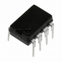
LM5021NA-1/NOPB National Semiconductor, LM5021NA-1/NOPB Datasheet

LM5021NA-1/NOPB
Specifications of LM5021NA-1/NOPB
*LM5021NA-1/NOPB
*LM5021NA-1NOPB
LM5021NA-1
LM5021NA-1NOPB
LM5021NA-1NOPB
Available stocks
Related parts for LM5021NA-1/NOPB
LM5021NA-1/NOPB Summary of contents
Page 1
... This high performance 8-pin IC has total propagation delays less than 100nS and a 1MHz capable oscillator that is programmed with a single resistor. Simplified Application Diagram © 2010 National Semiconductor Corporation LM5021 Features ■ Ultra Low Start-up Current (25 µA maximum) ■ ...
Page 2
... Order Number LM5021MM-1 80% Duty Cycle Limit LM5021MMX-1 80% Duty Cycle Limit LM5021NA-1 80% Duty Cycle Limit LM5021MM-2 50% Duty Cycle Limit LM5021MMX-2 50% Duty Cycle Limit LM5021NA-2 50% Duty Cycle Limit Pin Descriptions Pin Name Description 1 COMP Control input for the Pulse Width Modulator and Hiccup comparators. 2 VIN Input voltage ...
Page 3
... Absolute Maximum Ratings If Military/Aerospace specified devices are required, please contact the National Semiconductor Sales Office/ Distributors for availability and specifications. VIN to GND VIN Clamp Continuous Current CS to GND RT to GND All other pins to GND ESD Rating (Note 2) Human Body Model Storage Temperature ...
Page 4
Symbol Parameter PWM COMPARATOR COMP to OUT delay Min Duty Cycle Max Duty Cycle (-1 Device) Max Duty Cycle (-2 Device) COMP to PWM comparator gain COMP Open Circuit Voltage COMP at Max Duty Cycle COMP Short Circuit Current SLOPE ...
Page 5
Simplified Block Diagram FIGURE 1. 5 20144203 www.national.com ...
Page 6
Typical Performance Characteristics VIN Start-Up Current VIN Current vs OUT Load OUT Driver Current vs Temperature www.national.com Unless otherwise specified: T 20144204 VIN Voltage Falling vs VCC Voltage 20144206 Hiccup Mode Deadtime vs Softstart Capacitance 20144208 6 = 25°C. J ...
Page 7
Output Switching Frequency vs RT Detailed Operating Description START UP CIRCUIT Referring to Figure 2, the input capacitor C charged through the start-up resistor Rstart, when the recti- fied ac input voltage HV is applied. The VIN current consumed by ...
Page 8
RELATIONSHIP BETWEEN INPUT CAPACITOR C V CAPACITOR C CC VCC The internal VCC linear regulator is enabled when VIN reach- es 20V. The drop in VIN due to charge transfer from C C after the regulator is enabled can be ...
Page 9
LM5021-1: LM5021-2: The LM5021 can also be synchronized to an external clock. The external clock must have a higher frequency than the free running oscillator frequency set by the RT resistor. The clock signal should be capacitively coupled into the ...
Page 10
FIGURE 4. Waveform at SS and COMP Pin due to Continuous Overload www.national.com FIGURE 3. Hiccup Mode Control 10 20144219 20144220 ...
Page 11
FIGURE 5. Waveform at SS and COMP Pin due to Brief Overload SKIP CYCLE OPERATION During light load conditions, the efficiency of the switching power supply typically drops as the losses associated with switching and operating bias currents of the ...
Page 12
Typical Application Circuit www.national.com 12 ...
Page 13
Physical Dimensions inches (millimeters) unless otherwise noted 8 Lead MSOP Package NS Package Number MUA08A 8 Lead MDIP Package NS Package Number N08E 13 www.national.com ...
Page 14
... For more National Semiconductor product information and proven design tools, visit the following Web sites at: www.national.com Products Amplifiers www.national.com/amplifiers Audio www.national.com/audio Clock and Timing www.national.com/timing Data Converters www.national.com/adc Interface www.national.com/interface LVDS www.national.com/lvds Power Management www.national.com/power Switching Regulators www.national.com/switchers LDOs www.national.com/ldo LED Lighting www ...


