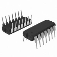
MC34060APG ON Semiconductor, MC34060APG Datasheet

MC34060APG
Specifications of MC34060APG
Available stocks
Related parts for MC34060APG
MC34060APG Summary of contents
Page 1
MC34060A, MC33060A Fixed Frequency, PWM, Voltage Mode Single Ended Controllers The MC34060A is a low cost fixed frequency, pulse width modulation control circuit designed primarily for single−ended SWITCHMODEt power supply control. The MC34060A is specified over the commercial operating temperature ...
Page 2
MAXIMUM RATINGS (Full operating ambient temperature range applies, unless otherwise noted.) Rating Power Supply Voltage Collector Output Voltage Collector Output Current (Note 3) Amplifier Input Voltage Range Power Dissipation @ T ≤ 45°C A Operating Junction Temperature Storage Temperature Range ...
Page 3
ELECTRICAL CHARACTERISTICS for min/max values T is the operating ambient temperature range that applies, unless otherwise noted.) A Characteristics REFERENCE SECTION Reference Voltage (I = 1.0 mA, T 25° − MC34060A A low ...
Page 4
ELECTRICAL CHARACTERISTICS (continued) For typical values T = 25°C, for min/max values T A Characteristics PWM COMPARATOR SECTION (Test circuit Figure 11) Input Threshold Voltage (Zero Duty Cycle) Input Sink Current (V = 0.7 V) [Pin 3] DEAD−TIME CONTROL SECTION ...
Page 5
Dead-Time Control + Error Amp 1 Description The MC34060A is a fixed−frequency pulse width modulation control circuit, incorporating the primary building blocks required for the control of a switching ...
Page 6
The control signals are external inputs that can be fed into the dead−time control, the error amplifier inputs, or the feed−back input. The dead−time control comparator has an effective 120 mV input offset which limits the minimum output dead time ...
Page 7
I , EMITTER CURRENT (mA) E Figure 7. Emitter−Follower Configuration Output Saturation Voltage versus Emitter Current 10 9.0 8.0 7.0 6.0 5.0 4.0 3.0 2.0 1.0 0 ...
Page 8
Error Amplifier + Under Test Other Error ref Amplifier Figure 11. Error Amplifier Characteristics 15V R L 68W C C Output L 15pF Transistor E 90% 90 10% 10 ...
Page 9
Output Voltage of System ref Positive Output Voltage ref Figure 15. Error Amplifier Sensing Techniques V ref Output T ...
Page 10
V = 8.0V to 40V in 0.01 47k 1.0M + 50/50 0.01 4.7k 4.7k 150 Test Line Regulation Load Regulation Output Ripple Short Circuit Current Efficiency Figure 19. Step−Down Converter with Soft−Start Tip ...
Page 11
V = 8.0V to 26V in 22k 0.05 33k 4.7k 2.7M + 50/35V 3.9k Test Line Regulation Load Regulation Output Ripple Efficiency *Optional circuit to minimize output ripple 150mH @ 4. ...
Page 12
V = 8.0V to 40V in 30k 0.01 47k 7.5k 1.0M + 50/50V 0.01 10k 47k 3.3k Test Line Regulation Load Regulation Output Ripple Short Circuit Current Efficiency *Optional circuit to minimize output ripple Figure 21. Step−Up/Down Voltage Inverting Converter ...
Page 13
http://onsemi.com 13 ...
Page 14
... ORDERING INFORMATION Operating Temperature Range Device MC34060ADG MC34060ADR2G T = 0° to +70°C A MC34060APG MC33060ADG MC33060ADR2G T = −40° to +85°C A MC33060APG †For information on tape and reel specifications, including part orientation and tape sizes, please refer to our Tape and Reel Packaging Specifications Brochure, BRD8011/D. ...
Page 15
... G −T− SEATING 14 PL PLANE 0.25 (0.010 14X 0.58 *For additional information on our Pb−Free strategy and soldering details, please download the ON Semiconductor Soldering and Mounting Techniques Reference Manual, SOLDERRM/D. PACKAGE DIMENSIONS SOIC−14 CASE 751A−03 ISSUE 0.25 (0.010 ...
Page 16
... Opportunity/Affirmative Action Employer. This literature is subject to all applicable copyright laws and is not for resale in any manner. PUBLICATION ORDERING INFORMATION LITERATURE FULFILLMENT: Literature Distribution Center for ON Semiconductor P.O. Box 5163, Denver, Colorado 80217 USA Phone: 303−675−2175 or 800−344−3860 Toll Free USA/Canada Fax: 303− ...


