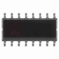
L6725TR STMicroelectronics, L6725TR Datasheet - Page 14

L6725TR
Manufacturer Part Number
L6725TR
Description
IC CTRLR PWM ADJ STP DWN 16SOICN
Manufacturer
STMicroelectronics
Datasheet
1.L6725ATR.pdf
(32 pages)
Specifications of L6725TR
Pwm Type
Voltage Mode
Number Of Outputs
1
Frequency - Max
550kHz
Duty Cycle
100%
Voltage - Supply
4.5 V ~ 18 V
Buck
Yes
Boost
No
Flyback
No
Inverting
No
Doubler
No
Divider
No
Cuk
No
Isolated
No
Operating Temperature
-40°C ~ 85°C
Package / Case
16-SOIC (3.9mm Width)
Frequency-max
550kHz
Output Voltage
0.6 V to 18 V
Output Current
30 A
Maximum Operating Temperature
+ 85 C
Minimum Operating Temperature
- 40 C
Mounting Style
SMD/SMT
For Use With
497-5867 - EVAL BOARD 20A 250KHZ L6725497-5500 - EVAL BOARD FOR L6725
Lead Free Status / RoHS Status
Lead free / RoHS Compliant
Other names
497-5096-2
Available stocks
Company
Part Number
Manufacturer
Quantity
Price
Part Number:
L6725TR
Manufacturer:
ST
Quantity:
20 000
Device description
5.7
5.8
Figure 8.
14/32
Driver section
The high-side and low-side drivers allow using different types of power MOSFETs (also multiple
MOSFETs to reduce the R
supplied by V
time control avoids MOSFETs cross-conduction maintaining very short dead time duration in
the range of 20ns. The control monitors the phase node in order to sense the low-side body
diode recirculation. If the phase node voltage is less than a certain threshold (-350mV typ.)
during the dead time, it will be reduced in the next PWM cycle. The predictive dead time control
doesn’t work when the high-side body diode is conducting because the phase node doesn’t go
negative. This situation happens when the converter is sinking current for example and, in this
case, an adaptive dead time control operates.
Monitoring and protections
The output voltage is monitored by means of pin FB. The device provides over-voltage-
protection: when the voltage sensed on FB pin reaches a value 20% (typ.) greater than the
reference the low-side driver is turned on as long as the over voltage is detected (see
The device realizes the over-current-protection (OCP) sensing the current both on the high-side
MOSFET(s) and the low-side MOSFET(s) and so 2 current limit thresholds can be set (see
OCH pin and OCL pin in
●
●
The Peak Current Protection is active when the high-side MOSFET(s) is turned on, after a
masking time of 100ns. The valley-current-protection is enabled when the low-side MOSFET(s)
is turned on after a masking time of 500ns. If, when the soft-start phase is completed, an over
current event occurs during the on time (peak-current-protection) or during the off time (valley-
current-protection) the device enters in HICCUP mode: the high-side and low-side MOSFET(s)
are turned off, the soft-start capacitor is discharged with a constant current of 10µA and when
the voltage at the SS pin reaches 0.5V the soft-start phase restarts (see
OVP
Peak Current Limit
Valley Current Limit
CCDR
while the high-side driver is supplied by the BOOT pin. A predictive dead
Table 4: Pin
DSON
), maintaining fast switching transitions. The low-side driver is
functions):
LGate
FB
Figure
L6725 - L6725A
9).
Figure
8).


