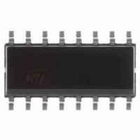
L6725 STMicroelectronics, L6725 Datasheet - Page 7

L6725
Manufacturer Part Number
L6725
Description
IC CTRLR PWM W/BOOTSTRAP SO-16N
Manufacturer
STMicroelectronics
Datasheet
1.L6725ATR.pdf
(32 pages)
Specifications of L6725
Pwm Type
Voltage Mode
Number Of Outputs
1
Frequency - Max
550kHz
Duty Cycle
100%
Voltage - Supply
4.5 V ~ 18 V
Buck
Yes
Boost
No
Flyback
No
Inverting
No
Doubler
No
Divider
No
Cuk
No
Isolated
No
Operating Temperature
-40°C ~ 85°C
Package / Case
16-SOIC (3.9mm Width)
Frequency-max
550kHz
Package
SO16N
For Use With
497-5867 - EVAL BOARD 20A 250KHZ L6725497-5500 - EVAL BOARD FOR L6725
Lead Free Status / RoHS Status
Lead free / RoHS Compliant
Available stocks
Company
Part Number
Manufacturer
Quantity
Price
Company:
Part Number:
L6725A
Manufacturer:
STMicroelectronics
Quantity:
135
Part Number:
L6725ATR
Manufacturer:
ST
Quantity:
20 000
Part Number:
L6725TR
Manufacturer:
ST
Quantity:
20 000
L6725 - L6725A
Table 4.
Pin n°
10
11
12
13
14
15
16
5
6
7
8
9
Pin functions
(L6725A)
(L6725A)
PGOOD
SYNCH
PHASE
(L6725)
(L6725)
HGATE
LGATE
V
PGND
SGND
BOOT
Name
OCH
N.C.
N.C.
V
CCDR
FB
CC
A resistor connected from this pin and the high-side MOSFET(s) drain sets the peak-
current-limit. The peak current is sensed through the high-side MOSFET(s). The
internal 100µA current generator (I
external resistor (R
equation:
This pin is connected to the source of the high-side MOSFET(s) and provides the
return path for the high-side driver. This pin monitors the drop across both the upper
and lower MOSFET(s) for the current limit together with OCH and OCL.
This pin is connected to the high-side MOSFET(s) gate.
Through this pin is supplied the high-side driver. Connect a capacitor from this pin to
the PHASE pin and a diode from V
This pin has to be connected closely to the low-side MOSFET(s) source in order to
reduce the noise injection into the device.
This pin is connected to the low-side MOSFET(s) gate.
5V internally regulated voltage. It is used to supply the internal drivers. Filter it to
ground with a 1uF ceramic cap.
Supply voltage pin. The operative supply voltage range is from 4.5V to 14V.
In L6725 this pin is N.C. With L6725A this pin is an open collector output and it is
pulled low if the output voltage is not
within the specified thresholds (90%-110%). If not used it may be left floating. Pull-up
this pin to V
In L6725 this pin is N.C. With L6725A it is a Master-Slave pin. Two or more devices
can be synchronized by simply
connecting the SYNCH pins together. The device operating with the highest FSW will
be the Master. The Slave devices will operate with 180° phase shift from the Master.
The best way to synchronize devices together is to set their FSW at the same value. If
it is not used the SYNCH pin can be left floating.
All the internal references are referred to this pin.
This pin is connected to the error amplifier inverting input. Connect it to V
the compensation network. This pin is also used to sense the output voltage in order
to manage the over voltage protection.
CCDR
with a 10K resistor to obtain a logical signal.
OCH
). The over-current threshold is given by the following
I
PEAK
OCH
CCDR
Function
) sinks a current from the drain through the
=
I
OCH
to this pin (cathode versus BOOT).
R
DSonHS
⋅
R
OCH
Pin connections and functions
OUT
through
7/32


