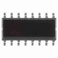
L6725A STMicroelectronics, L6725A Datasheet - Page 4

L6725A
Manufacturer Part Number
L6725A
Description
IC PWM CTLR VOLTAGE MODE SO-16N
Manufacturer
STMicroelectronics
Datasheet
1.L6725ATR.pdf
(32 pages)
Specifications of L6725A
Pwm Type
Voltage Mode
Number Of Outputs
1
Frequency - Max
550kHz
Duty Cycle
100%
Voltage - Supply
4.5 V ~ 18 V
Buck
Yes
Boost
No
Flyback
No
Inverting
No
Doubler
No
Divider
No
Cuk
No
Isolated
No
Operating Temperature
-40°C ~ 85°C
Package / Case
16-SOIC (3.9mm Width)
Frequency-max
550kHz
Output Voltage
0.603 V
Input Voltage
1.8 V to 18 V
Switching Frequency
500 KHz
Operating Temperature Range
- 40 C to + 125 C
Mounting Style
SMD/SMT
Duty Cycle (max)
100 %
Package
SO16N
For Use With
497-5867 - EVAL BOARD 20A 250KHZ L6725497-5500 - EVAL BOARD FOR L6725
Lead Free Status / RoHS Status
Lead free / RoHS Compliant
Available stocks
Company
Part Number
Manufacturer
Quantity
Price
Company:
Part Number:
L6725A
Manufacturer:
STMicroelectronics
Quantity:
135
Part Number:
L6725ATR
Manufacturer:
ST
Quantity:
20 000
Summary description
1
1.1
4/32
Summary description
The device is a flexible high performance PWM buck controller dedicated for low voltage
distributed DC-DC. The input voltage can range from 1.8V to 18V, while the supply voltage can
range from 4.5V to 18V. The output voltage is adjustable down to 0.6V.
High peak current gate drivers provide for fast switching to the external power section, and the
output current can be in excess of 20A. The device is capable to manage minimum on-times
(T
switching frequency. In order to guarantee a real overcurrent protection, also with very narrow
T
necessary, two different current limit protections can be externally set through an external
resistor. The device can sink current after the soft-start phase while, during the soft-start, the
sink mode capability is disabled in order to allow a proper start-up also in pre-biased output
voltage conditions. Other features are over-voltage-protection and thermal shutdown.
Functional description
Figure 1.
ON
ON
, the current sense is realized both on the high-side and low-side MOSFETs. When
) shorter than 100ns making possible conversions with very low duty cycle and very high
PGOOD
EAREF
EAREF
SYNCH
SS
SS
Block diagram
Protection and Ref
Protection and Ref
OCL
OCL
Monitor
Monitor
+
+
-
-
0.6V
Vcc=4.5V-14V
OCH
OCH
Vcc = 14V - 18V
OSC
OSC
L6725
LDO
LDO
FB
FB
+
+
-
-
+
+
+
VCCDR
VCCDR
PWM
PWM
-
-
-
E/A
E/A
-
-
COMP
COMP
BOOT
BOOT
HGATE
HGATE
PHASE
PHASE
LGATE
LGATE
PGND
PGND
GND
GND
Vin = 14V - 18V
Vin=1.8V-14V
L6725 - L6725A
V
OUT


