ISL6269CRZ Intersil, ISL6269CRZ Datasheet

IC CTRLR PWM 1-PHASE GPU 16-QFN

ISL6269CRZ

Manufacturer Part Number
ISL6269CRZ
Description
IC CTRLR PWM 1-PHASE GPU 16-QFN
Manufacturer
Intersil
Datasheet

Specifications of ISL6269CRZ

Pwm Type
Controller
Number Of Outputs
1
Frequency - Max
600kHz
Voltage - Supply
7 V ~ 25 V
Buck
Yes
Boost
No
Flyback
No
Inverting
No
Doubler
No
Divider
No
Cuk
No
Isolated
No
Operating Temperature
-10°C ~ 100°C
Package / Case
16-VQFN Exposed Pad, 16-HVQFN, 16-SQFN, 16-DHVQFN
Frequency-max
600kHz
Lead Free Status / RoHS Status
Lead free / RoHS Compliant
Duty Cycle
-

Available stocks

Company
Part Number
Manufacturer
Quantity
Price
Part Number:
ISL6269CRZ
Manufacturer:
INTERSIL
Quantity:
17
Part Number:
ISL6269CRZ
Manufacturer:
INTERSIL
Quantity:
20 000
Part Number:
ISL6269CRZ-T
Manufacturer:
INTERSIL/PBF
Quantity:
5 999
Part Number:
ISL6269CRZ-T
Manufacturer:
INTERSIL
Quantity:
20 000
High-Performance Notebook PWM
Controller with Bias Regulator and
Audio-Frequency Clamp
The ISL6269 IC is a Single-Phase Synchronous-Buck PWM
controller featuring Intersil's Robust Ripple Regulator (R
technology that delivers truly superior dynamic response to
input voltage and output load transients. Integrated
MOSFET drivers, 5V LDO and bootstrap diode result in
fewer components and smaller implementation area.
Intersil’s R
frequency PWM and hysteretic PWM while eliminating many
of their shortcomings. R
modulator that synthesizes an AC ripple voltage signal V
analogous to the output inductor ripple current. The AC signal
V
the error amplifier output V
programmable voltage reference V
of the PWM signal. The voltage reference V
state PWM frequency. Both edges of the PWM can be
modulated in response to input voltage transients and output
load transients, much faster than conventional fixed frequency
PWM controllers. Unlike a conventional hysteretic converter,
the ISL6269 has an error amplifier that provides ±1% voltage
regulation at the FB pin.
The ISL6269 has a 1.5ms digital soft-start and can be started
into a pre-biased output voltage. A resistor divider is used to
program the output voltage setpoint. The ISL6269 can be
configured to operate in continuous-conduction-mode (CCM)
or diode-emulation-mode (DEM), which improves light-load
efficiency. In CCM the controller always operates as a
synchronous rectifier however, when DEM is enabled the
low-side MOSFET is permitted to stay off, blocking negative
current flow into the low-side MOSFET from the output
inductor.
Pinout
R
enters a window comparator where the lower threshold is
3
FCCM
technology combines the best features of fixed-
VCC
VIN
EN
1
2
3
4
(16 LD 4x4 QFN)
16
5
3
technology employs an innovative
TOP VIEW
COMP
ISL6269
15
®
6
GND
1
, and the upper threshold is a
14
7
W,
13
Data Sheet
8
resulting in generation
12
10
11
9
W
PVCC
LG
PGND
ISEN
sets the steady
1-888-INTERSIL or 1-888-468-3774
R
3
,
)
CAUTION: These devices are sensitive to electrostatic discharge; follow proper IC Handling Procedures.
Features
• High performance R
• Fast transient response
• +0.6V Internal Reference
• Wide input voltage range: +7.0V to +25.0V
• Output voltage range: +0.6V to +3.3V
• Wide output load range: 0A to 25A
• Selectable diode emulation mode for increased light load
• Programmable PWM frequency: 200kHz to 600kHz
• Pre-biased output start-up capability
• Internal 5V LDO for self-biasing
• Integrated MOSFET drivers and bootstrap diode
• Internal digital soft-start
• Power good monitor
• PWM minimum frequency above audible spectrum
• Fault protection
• Pb-free (RoHS compliant)
Applications
• PCI express graphical processing unit
• Auxiliary power rail
• VRM
• Network adapter
Ordering Information
ISL6269CRZ*
ISL6269IRZ*
*Add “-T” suffix for tape and reel. Please refer to TB347 for details on
reel specifications.
NOTE: These Intersil Pb-free plastic packaged products employ
special Pb-free material sets, molding compounds/die attach
materials, and 100% matte tin plate plus anneal (e3 termination
finish, which is RoHS compliant and compatible with both SnPb and
Pb-free soldering operations). Intersil Pb-free products are MSL
classified at Pb-free peak reflow temperatures that meet or exceed
the Pb-free requirements of IPC/JEDEC J STD-020.
- ±0.6% tolerance over the commercial temperature
- ±1.0% tolerance over the industrial temperature range
efficiency
- Undervoltage protection
- Soft crowbar overvoltage protection
- Low-side MOSFET r
- Over-temperature protection
- Fault identification by PGOOD pull-down resistance
NUMBER
range (0°C to +70°C)
(-40°C to +85°C)
(Note)
PART
All other trademarks mentioned are the property of their respective owners.
June 25, 2009
|
Copyright Intersil Americas Inc. 2006, 2007, 2009. All Rights Reserved
Intersil (and design) is a registered trademark of Intersil Americas Inc.
62 69CRZ -10 to +100 16 Ld 4x4 QFN L16.4x4
62 69IRZ
MARKING
PART
3
technology
DS(ON)
-40 to +100 16 Ld 4x4 QFN L16.4x4
RANGE
TEMP
(°C)
overcurrent protection
PACKAGE
(Pb-free)
ISL6269
FN9177.3
DWG. #
PKG.

Related parts for ISL6269CRZ

ISL6269CRZ Summary of contents

Page 1

... Applications • PCI express graphical processing unit • Auxiliary power rail • VRM • Network adapter Ordering Information PART NUMBER (Note) ISL6269CRZ* PVCC 12 ISL6269IRZ* LG *Add “-T” suffix for tape and reel. Please refer to TB347 for details on 11 reel specifications. PGND ...

Page 2

Block Diagram VIN GND PACKAGE BOTTOM VCC V REF EN − OVP + − UVP + + EA EA − FB COMP − ISEN OCP 30Ω PGOOD 5V LDO + − ...

Page 3

Typical Application R PGOOD R PVCC C C PVCC VCC R COMP C COMP1 C COMP2 R BOTTOM 3 ISL6269 ISL6269 PGOOD VIN PVCC UG VCC BOOT GND PHASE FCCM ISEN EN LG COMP PGND FB FSET VO R TOP ...

Page 4

... Storage Temperature . . . . . . . . . . . . . . . . . . . . . . . .-65°C to +150°C Pb-Free Reflow Profile .see link below http://www.intersil.com/pbfree/Pb-FreeReflow.asp Recommended Operating Conditions Ambient Temperature Range ISL6269CRZ . . . . . . . . . . . . . . . . . . . . . . . . . . . .-10°C to +100°C ISL6269IRZ . . . . . . . . . . . . . . . . . . . . . . . . . . . . .-40°C to +100°C Supply Voltage (VIN to GND 25V PVCC to PGND . . . . . . . . . . . . . . . . . . . . . . . . . . . . . . . . . . .5V ±5% = -40°C to +100°C, unless otherwise stated. All typical specifications T ...

Page 5

Electrical Specifications These specifications apply for T PVCC = 5V, VIN = 15V. Parameters with MIN and/or MAX limits are 100% tested at +25°C, unless otherwise specified. Temperature limits established by characterization and are not production tested. (Continued) PARAMETER VO ...

Page 6

Electrical Specifications These specifications apply for T PVCC = 5V, VIN = 15V. Parameters with MIN and/or MAX limits are 100% tested at +25°C, unless otherwise specified. Temperature limits established by characterization and are not production tested. (Continued) PARAMETER FCCM ...

Page 7

... Theory of Operation Modulator The ISL6269 is a hybrid of fixed frequency PWM control, and variable frequency hysteretic control. Intersil’s R can simultaneously affect the PWM switching frequency and PWM duty cycle in response to input voltage and output load transients. The term “Ripple” in the name “Robust-Ripple- Regulator” ...

Page 8

When the EN pin is pulled above the rising EN threshold voltage V ENTHR ramped above the rising POR V VCC_THR the PGOOD Soft-Start Delay t starts and the output voltage SS begins to rise. The output ...

Page 9

PWM frequency characteristic of the R architecture for the PWM frequency to decrease while in diode emulation. The extent of the frequency reduction is proportional to the ...

Page 10

... GATE DRIVERS (EQ. 7) (EQ. 8) FIGURE 6. COMPENSATION REFERENCE CIRCUIT Your local Intersil representative can provide a PC-based tool that can be used to calculate compensation network component values and help simulate the loop frequency response. The compensation network consists of the internal should be checked error amplifier of the ISL6269 and the external components R1, ...

Page 11

... Intersil provides complete reference designs that include schematics, bills of materials, and example board layouts. Selecting the LC Output Filter The duty cycle of an ideal buck converter is a function of the input and the output voltage. This relationship is written as: V OUT ...

Page 12

MOSFET Selection and Considerations Typically, a MOSFET cannot tolerate even brief excursions beyond their maximum drain to source voltage rating. The MOSFETs used in the power stage of the converter should have a maximum V rating that exceeds the sum ...

Page 13

... Accordingly, the reader is cautioned to verify that data sheets are current before placing orders. Information furnished by Intersil is believed to be accurate and reliable. However, no responsibility is assumed by Intersil or its subsidiaries for its use; nor for any infringements of patents or other rights of third parties which may result from its use ...

Page 14

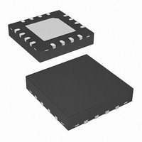
Package Outline Drawing L16.4x4 16 LEAD QUAD FLAT NO-LEAD PLASTIC PACKAGE Rev 6, 02/08 4.00 6 PIN 1 INDEX AREA 0.15 (4X) TOP VIEW ( TYP ) ( TYPICAL RECOMMENDED LAND PATTERN 14 ...

Related keywords