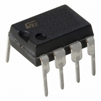
E-UC3845BN STMicroelectronics, E-UC3845BN Datasheet

E-UC3845BN
Specifications of E-UC3845BN
Related parts for E-UC3845BN
E-UC3845BN Summary of contents
Page 1
... The UC3842B and UC3844B have UVLO thresholds of 16V (on) and 10V (off), ideally suited off-line applications The corresponding thresh- olds for the UC3843B and UC3845B are 8.5 V and 7.9 V. The UC3842B and UC3843B can operate to duty cycles approaching 100%. A range of the zero to < ...
Page 2
... T resistor GROUND This pin is the combined control circuitry and power ground. 6 OUTPUT This output directly drives the gate of a power MOSFET. Peak currents are sourced and sunk by this pin This pin is the positive supply of the control IC This is the reference output. It provides charging current for capacitor C ...
Page 3
... THERMAL DATA Symbol R Thermal Resistance Junction-ambient. th j-amb ELECTRICAL CHARACTERISTICS ( [note 1] Unless otherwise stated, these specifications apply for -25 < T < for UC284XB; 0 < T amb Symbol Parameter REFERENCE SECTION V Output Voltage REF Line Regulation V REF Load Regulation V REF / T Temperature Stability V REF Total Output Variation ...
Page 4
... Operating Supply Current i V Zener Voltage iz Notes : 1. Max package power dissipation limits must be respected; low duty cycle pulse techniques are used during test maintain T close possible. amb 2. These parameters, although guaranteed, are not 100% tested in production. 3. Parameter measured at trip point of latch with V 4 ...
Page 5
... UC2842B/3B/4B/5B - UC3842B/3B/4B/ REF COMP UC2842B I SENSE pin single point ground. The transistor and 5 K potentiometer are used to sample the oscillator waveform and apply an adjustable ramp to pin 3. Figure 3: Output Dead-Time vs. Oscillator Fre- D95IN333 % 200K 300K 500K f (KHz) 10K OSC A 0 0.1 F ...
Page 6
... Figure 5: Maximum Output Duty Cycle vs. Tim- D95IN335 D max (%) =15V i 90 =2V OSC 100 T (˚C) A Figure 7: Current Sense Input Threshold vs. Er- V D95IN337 (V) = 1.0 =100K =25˚C 60 0.8 90 0.6 Phase 120 0.4 150 0.2 180 0.0 1M f(Hz) Figure 9: Reference Short Circuit Current vs. ...
Page 7
... Sink Saturation (Load 200 400 Figure 12: Output Waveform. 90% 10% 50ns/DIV Figure 14: Oscillator and Output Waveforms. 8 PWM R T CLOCK UC2842B/3B/4B/5B - UC3842B/3B/4B/5B Figure 11: Supply Current vs. Supply Voltage D95IN341 (mA) T =-40˚ =25˚ GND 0 600 I (mA) O Figure 13: Output Cross Conduction V =15V 1.0nF L = 25°C ...
Page 8
... Figure 16 : Under Voltage Lockout. 7 ON/OFF COMMAND OFF Figure 17 : Current Sense Circuit . CURRENT D95IN347 Peak current ( determined by the formula s 1 max small RC filter may be required to suppress switch transients. 8/15 2. COMP REST OF IC <17mA UC3842B UC3843B UC3844B UC3845B 16V 8.4V <0.5mA 10V 7.6V ERROR AMPL. 1 COMP 3 ...
Page 9
... Figure 18 : Slope Compensation Techniques. V REG SLOPE SENSE R S Figure 19 : Isolated MOSFET Drive and Current Transformer Sensing 5.0V ref - + - COMP/LATCH UC2842B/3B/4B/5B - UC3842B/3B/4B/ UC3842B GND ISOLATION BOUNDARY D95IN349 V REG UC3842B C T SLOPE SENSE Waveforms 50 -1.4 (pin GND D95IN348 - 25 9/15 ...
Page 10
... UC2842B/3B/4B/5B - UC3842B/3B/4B/5B Figure 20 : Latched Shutdown. 2N 3905 SCR must be selected for a holding current of less than 0.5mA at T The simple two transistor circuit can be used in place of the SCR as shown. All resistors are 10K. Figure 21: Error Amplifier Compensation From Error Amp compensation circuit for stabilizing any current-mode topology except for boost and flyback converters operating with continuous inductor current ...
Page 11
... Figure 22: External Clock Synchronization. EXTERNAL SYNC INPUT 0.01 F The diode clamp is required if the Sync amplitude is large enough to cause the bottom side of C Figure 23: External Duty Cycle Clamp and Multi Unit Synchronization. V REF 1. max ( UC2842B/3B/4B/5B - UC3842B/3B/4B/5B V REF more than 300mV below ground ...
Page 12
... UC2842B/3B/4B/5B - UC3842B/3B/4B/5B Figure 24: Soft-Start Circuit Figure 25: Soft-Start and Error Amplifier Output Duty Cycle Clamp BC109 V CLAMP 12/15 R BIAS R OSC + 1mA BIAS - R OSC + 1mA V Clamp · = where 0 <V <1V CLAMP ref + - D95IN354 ref - Comp/Latch V CLAMP I = D95IN355 pk(max ...
Page 13
... F (1) 3.8 4.0 L 0.4 1.27 0.016 M 0 (max.) (1) D and F do not include mold flash or protrusions. Mold flash or potrusions shall not exceed 0.15mm (.006inch). UC2842B/3B/4B/5B - UC3842B/3B/4B/5B inch TYP. MAX. 0.069 0.010 0.065 0.033 0.019 0.010 0.020 0.197 0.244 0.050 ...
Page 14
... D 10.92 E 7.95 9.75 0.313 e 2.54 e3 7.62 e4 7.62 F 6.6 I 5.08 L 3.18 3.81 0.125 Z 1.52 14/15 inch MIN. TYP. MAX. 0.131 0.065 0.022 0.012 0.430 0.384 0.100 0.300 0.300 0.260 0.200 0.150 0.060 OUTLINE AND MECHANICAL DATA Minidip ...
Page 15
... The ST logo is a registered trademark of STMicroelectronics © 1999 STMicroelectronics – Printed in Italy – All Rights Reserved Australia - Brazil - Canada - China - France - Germany - Italy - Japan - Korea - Malaysia - Malta - Mexico - Morocco - The Netherlands - Singapore - Spain - Sweden - Switzerland - Taiwan - Thailand - United Kingdom - U.S.A. UC2842B/3B/4B/5B - UC3842B/3B/4B/5B STMicroelectronics GROUP OF COMPANIES http://www ...


