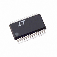
LTC3714EG#PBF Linear Technology, LTC3714EG#PBF Datasheet

LTC3714EG#PBF
Specifications of LTC3714EG#PBF
Available stocks
Related parts for LTC3714EG#PBF
LTC3714EG#PBF Summary of contents
Page 1
... In shutdown, the device draws <1µA. L, LT, LTC, LTM and Burst Mode are registered trademarks and Hot Swap and ThinSOT are trademarks of Linear Technology Corporation. All other trademarks are the property of their respective owners. Protected by U.S. Patents including 5481178, 6580258, 6304066, 6127815, 6498466, 6611131, 6144194 ...
Page 2
LTC3417A absoluTe MaxiMuM raTings Voltages ...................................... – 0. IN1 IN2 SYNC/MODE, SW1, SW2, RUN1, RUN2 PHASE, FREQ, FB1 FB2 Voltages............... – 0. TH1 TH2 V – ...
Page 3
T SYMBOL PARAMETER I Input DC Supply Current (Note 4) S Active Mode Half Active Mode (V = 0V, 1.5A Only) RUN2 Half Active Mode (V = 0V, 1A Only) RUN1 Both ...
Page 4
LTC3417A Typical perForMance characTerisTics OUT1 Burst Mode Operation V OUT 20mV/DIV I L 250mA/DIV V = 3.6V 2µs/DIV 1.8V OUT I = 100mA LOAD REFER TO FIGURE 4 OUT2 Burst Mode Operation V OUT 20mV/DIV I L ...
Page 5
Typical perForMance characTerisTics OUT2 Efficiency (Pulse Skipping Mode) 100 I = 250mA LOAD 800mA LOAD 2.5V OUT REFER TO FIGURE 2.5 3 3.5 4 4.5 ...
Page 6
LTC3417A pin FuncTions (DFN/TSSOP) RUN1 (Pin 1/Pin 2): Enable for 1.5A Regulator. When at Logic 1, 1.5A regulator is running. When at 0V, 1.5A regulator is off. When both RUN1 and RUN2 are at 0V, the part is in shutdown. ...
Page 7
FuncTional DiagraM 1.5A REGULATOR V FB1 0.752V 0.848V RUN1 VOLTAGE REFERENCE RUN2 SYNC/MODE 0.848V 0.752V V FB2 1A REGULATOR I TH1 I TH LIMIT + – – – + LOGIC – V IN2 – LOGIC + ...
Page 8
LTC3417A operaTion The LTC3417A uses a constant frequency, current mode architecture. Both channels share the same clock frequency. The PHASE pin sets whether the channels are running in-phase or out of phase. The operating frequency is de- termined by connecting ...
Page 9
A general LTC3417A application circuit is shown in Figure 4. External component selection is driven by the load requirement, and begins with the selection of the inductors L1 and L2. Once L1 and L2 are chosen ...
Page 10
LTC3417A applicaTions inForMaTion Inductor Core Selection Different core materials and shapes will change the size/ current relationship of an inductor. Toroid or shielded pot cores in ferrite or permalloy materials are small and don’t radiate much energy, but generally cost ...
Page 11
When then the equation simplifies to 1– RMS – OUT OUT ...
Page 12
LTC3417A applicaTions inForMaTion is given to ripple current ratings and long term reliability. Ceramic capacitors have the lowest ESR and cost but also have the lowest capacitance density, high voltage and temperature coefficient and exhibit audible piezoelectric effects. In addition, ...
Page 13
V RUN 2V/DIV V OUT 1V/DIV I L 1A/DIV V = 3.6V 200µs/DIV 1.8V OUT R = 0.9 L Figure 2. Digital Soft-Start OUT1 I over 1024 clock cycles, as can be seen in Figures ...
Page 14
... For a detailed explanation of optimizing the compensation components, including a review of control loop theory, refer to Linear Technology Application Note 76. Although a buck regulator is capable of providing the full output current in dropout, it should be noted that as the ...
Page 15
V to ground. The resulting charge over the switching IN period is a current out of V that is typically much larger IN than the DC ...
Page 16
LTC3417A applicaTions inForMaTion Remembering that the above junction temperature is obtained from 25°C, we might recalculate DS(ON) the junction temperature based on a higher R it increases with temperature. However, we can safely as- sume that the ...
Page 17
V IN 2.25V TO 5.5V V OUT1 1.8V C1 22pF 1.5A R1 511k C OUT1 47µF L1: MIDCOM DUS-5121-1R5R C : KEMET C1210C226K8PAC OUT1 Figure 4. 1.8V at 1.5A/2. Step-Down Regulators ...
Page 18
LTC3417A applicaTions inForMaTion Board Layout Considerations When laying out the printed circuit board, the following checklist should be used to ensure proper operation of the LTC3417A. These items are also illustrated graphically in the layout diagram of Figure 5. Check ...
Page 19
DescripTion 3.50 ±0.05 1.65 ±0.05 2.20 ±0.05 (2 SIDES) RECOMMENDED SOLDER PAD PITCH AND DIMENSIONS PIN 1 TOP MARK (SEE NOTE 6) 0.200 REF NOTE: 1. DRAWING PROPOSED TO BE MADE VARIATION OF VERSION (WJED-1) IN JEDEC PACKAGE OUTLINE ...
Page 20
LTC3417A package DescripTion 6.60 ±0.10 4.50 ±0.10 SEE NOTE 4 RECOMMENDED SOLDER PAD LAYOUT 4.30 – 4.50* (.169 – .177) 0.09 – 0.20 0.50 – 0.75 (.0035 – .0079) (.020 – .030) NOTE: 1. CONTROLLING DIMENSION: MILLIMETERS 2. DIMENSIONS ARE ...
Page 21
... Changed 100µA to 125µA in the last paragraph of the Description section. Information furnished by Linear Technology Corporation is believed to be accurate and reliable. However, no responsibility is assumed for its use. Linear Technology Corporation makes no representa- tion that the interconnection of its circuits as described herein will not infringe on existing patent rights. ...
Page 22
... V = 0.8V 380µA, IN OUT(MIN 2.5V to 5.5V 2.4V 25µA, IN OUT(MIN 2.5V to 5.5V 2.4V 25µA, IN OUT(MIN 2.4V to 5.5V 2.4V 28µA, IN OUT(MIN 2.5V to 5.5V 0.6V 32µA, IN OUT(MIN 2.5V to 5.5V 0.6V 40µA, IN OUT(MIN) Q 3417afc LT 0311 REV C • PRINTED IN USA LINEAR TECHNOLOGY CORPORATION 2006 ...


