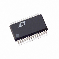
LTC3714EG#PBF Linear Technology, LTC3714EG#PBF Datasheet - Page 13

LTC3714EG#PBF
Manufacturer Part Number
LTC3714EG#PBF
Description
IC STP-DWN CNTRLR W/OPAMP 28SSOP
Manufacturer
Linear Technology
Datasheet
1.LTC3714EGPBF.pdf
(22 pages)
Specifications of LTC3714EG#PBF
Applications
Controller, Intel Pentium®
Voltage - Input
4 ~ 36 V
Number Of Outputs
1
Voltage - Output
0.6 ~ 1.75 V
Operating Temperature
-40°C ~ 85°C
Mounting Type
Surface Mount
Package / Case
28-SSOP
Primary Input Voltage
36V
No. Of Outputs
1
Output Voltage
1.75V
Output Current
20A
No. Of Pins
28
Operating Temperature Range
-40°C To +85°C
Msl
MSL 1 - Unlimited
Rohs Compliant
Yes
Lead Free Status / RoHS Status
Lead free / RoHS Compliant
Available stocks
Company
Part Number
Manufacturer
Quantity
Price
applicaTions inForMaTion
I
and 3. As the voltage on I
range, the internal peak current limit is also ramped at a
proportional linear rate.
Mode Selection
The SYNC/MODE pin is a multipurpose pin which provides
mode selection and frequency synchronization. Connect-
ing this pin to V
regulators, which provides the best low current efficiency
at the cost of a higher output voltage ripple. When SYNC/
MODE is connected to ground, pulse skipping operation
is selected for both regulators, which provides the lowest
output voltage and current ripple at the cost of low cur-
rent efficiency. Applying a voltage that is more than 1V
from either supply results in forced continuous mode for
both regulators, which creates a fixed output ripple and
allows the sinking of some current (about 1/2∆I
the switching noise is constant in this mode, it is also the
easiest to filter out. In many cases, the output voltage
can be simply connected to the SYNC/MODE pin, select-
ing the forced continuous mode except at start-up. The
LTC3417A can also be synchronized to an external clock
signal by the SYNC/MODE pin. The internal oscillator fre-
quency should be set to 20% lower than the external clock
frequency to ensure adequate slope compensation, since
slope compensation is derived from the internal oscillator.
During synchronization, the mode is set to pulse skipping
TH
over 1024 clock cycles, as can be seen in Figures 2
2V/DIV
1V/DIV
1A/DIV
V
V
RUN
OUT
I
L
V
V
R
Figure 2. Digital Soft-Start OUT1
IN
OUT
L
IN
= 0.9
= 3.6V
= 1.8V
enables Burst Mode operation for both
200µs/DIV
TH
ramps through its operating
L
). Since
and the top switch turn-on is synchronized to the rising
edge of the external clock.
When using an external clock, with the PHASE pin low, the
switching of the two channels occur at the edges of the
external clock. A 50% duty cycle will therefore produce
180° out-of-phase operation.
Checking Transient Response
The I
to be optimized for a wide range of loads and output
capacitors. The availability of the I
optimization of the control loop behavior, but also pro-
vides a DC coupled and AC filtered closed-loop response
test point. The DC step, rise time, and settling at this test
point truly reflects the closed-loop response. Assuming a
predominantly second order system, phase margin and/or
damping factor can be estimated using the percentage of
overshoot seen at this pin. The bandwidth can also be
estimated using the percentage of overshoot seen at this
pin or by examining the rise time at this pin.
The I
will provide an adequate starting point for most applica-
tions. The series RC filter sets the dominant pole-zero
loop compensation. The values can be modified slightly
(from 0.5 to 2 times their suggested values) to optimize
transient response once the final PC layout is done and
the particular output capacitor type and value have been
TH
TH
0.5A/DIV
external components shown in the Figure 4 circuit
pin compensation allows the transient response
2V/DIV
1V/DIV
V
V
RUN
OUT
I
L
V
V
R
Figure 3. Digital Soft-Start OUT2
IN
OUT
L
= 2
= 3.6V
= 2.5V
200µs/DIV
TH
LTC3417A
pin not only allows
13
3417afc


